1、 When 'thin' becomes a hard constraint: the technical logic of thin film absorbing materials
Traditional absorbing materials (such as absorbing foam, absorbing rubber, etc.) typically have a thickness between 0.5mm and 5mm, relying on sufficient material thickness to establish impedance matching and loss paths. However, in devices such as smartphones, smartwatches, and foldable phones, the available internal space has been compressed to the level of 0.1mm-0.3mm - traditional absorbing materials simply cannot fit in.
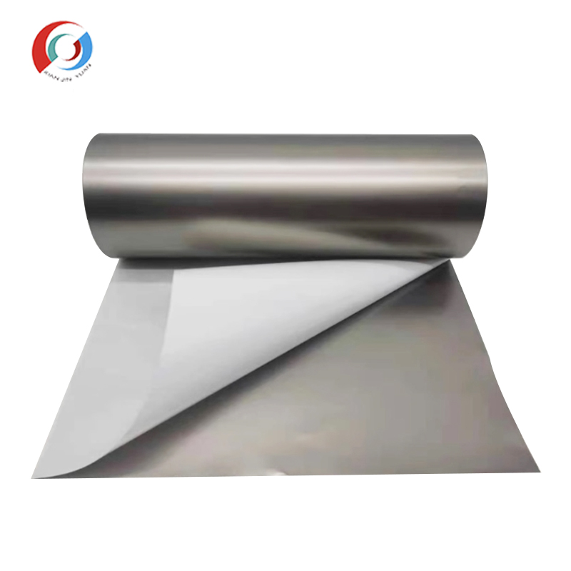
Thin film absorbing materials are born in response to this constraint. It uses polymer films (such as PET, PI, etc.) as substrates, and integrates the absorbing functional layer (magnetic filler/dielectric filler/conductive network) into a flexible film form with a thickness of only 0.03mm to 0.5mm through coating, sputtering, or composite processes. The core design concept can be summarized as: constructing an efficient electromagnetic wave absorption path within micrometer thickness.
To achieve this goal, two technical challenges need to be overcome. Impedance matching is the "ticket" to absorption - electromagnetic waves can only be effectively absorbed when they enter the interior of the material rather than being reflected on the surface. Thin film absorbing materials achieve gradual impedance matching with free space by precisely adjusting the electromagnetic parameters (dielectric constant and magnetic permeability) of the functional layer, thereby guiding electromagnetic waves to "enter" rather than "bounce". The loss ability is the "digestive system" of absorbing waves - electromagnetic waves entering the interior of materials need to be converted into thermal energy through dielectric loss or magnetic loss. Thin film absorbing materials typically use a composite system of magnetic fillers (such as carbonyl iron powder, iron silicon aluminum alloy, etc.) and dielectric fillers (such as carbon based materials) to construct multiple loss mechanisms within micrometer thickness.
2、 From laboratory to mass production: cutting-edge breakthroughs in thin film absorption technology
The technological progress of thin film absorbing materials is accelerating. In 2026, multiple cutting-edge research findings have revealed the direction of evolution in this field.
In terms of absorption efficiency, the electromagnetic absorption limit of non-magnetic conductive thin films has been redefined. The latest research has found that the electromagnetic absorption rate of non-magnetic conductive thin films can reach a new limit of about 82.8%, providing a new theoretical basis for the design of high-performance ultra-thin absorbing materials. This discovery means that even without relying on traditional magnetic materials, efficient absorption can be achieved through precise thin film structure design.
In terms of flexible integration, magnetic field assisted assembly strategy has been used for large-scale preparation of flexible metamaterial films with programmable strips or mesh arrays, achieving ultra wideband electromagnetic wave absorption, while the films have good flexibility and stretchability (stretchability up to three times their original length). This stretchable property gives it unique application value in flexible electronics and wearable devices.
In terms of multifunctional integration, liquid-liquid phase separation strategy is used to prepare flexible and repairable ultra wideband electromagnetic wave absorbing materials, which have high transparency (about 85%), strength and toughness (fracture strength of about 8.2 MPa), and excellent tensile properties (about 900% strain), with an electromagnetic wave absorption repair rate of up to 97%. The emergence of transparent absorbing films provides a new possibility for scenes such as display screens and optical windows that require both visual transparency and electromagnetic compatibility.
Advanced Institute Technology keeps up with academic frontiers and industry demands, and through continuous iteration of material formulas and coating processes, transforms laboratory level technological breakthroughs into engineering products that can be mass-produced and customized, providing customers with thin film absorbing material solutions with adjustable thickness, frequency band customization, and shape cutting.
3、 Three core application scenarios: from foldable screens to millimeter wave radar
Consumer electronics and wearable devices are the fields with the largest usage of thin-film absorbing materials. Smartphones, smartwatches, TWS earphones, AR/VR glasses and other devices have extremely limited internal space, but the electromagnetic environment is becoming increasingly complex - Bluetooth, WiFi, 5Gsub-6GHz, NFC and other multi-mode communications coexist in the same small space. The ultra-thin characteristics of thin film absorbing materials enable them to be attached to key parts such as processors, antennas, camera modules, display driver chips, etc., effectively suppressing near-field noise and cavity resonance without increasing thickness. In foldable smartphones, thin film absorbing materials also need to withstand repeated bending without performance degradation, which puts higher demands on the flexibility and fatigue life of the materials. Ultra thin flexible absorbing materials have been widely used in wearable devices, electromagnetic shielding coatings, and other fields.
5G/6G communication devices represent the most technically demanding application direction. The 5G millimeter wave and future 6G frequency bands have raised higher requirements for the frequency response of absorbing materials. The trend towards miniaturization and high integration of communication equipment has made electromagnetic radiation interference between internal modules of base stations a key challenge affecting equipment stability. Thin film absorbing materials can be used inside components such as base station antennas, RF front-end modules, filters, etc., to suppress resonance and reduce noise by absorbing stray electromagnetic waves inside the cavity. In the 5G millimeter wave frequency band, thin film absorbing materials with broadband absorption characteristics are becoming the preferred choice for base station equipment manufacturers.
Automotive electronics and intelligent driving are the fastest-growing application directions. The millimeter wave radar (24GHz, 77GHz and other frequency bands), laser radar and vehicle communication module in advanced driving assistance systems have extremely strict requirements for electromagnetic compatibility. Thin film absorbing materials can be used inside radar modules to suppress cavity resonance and reduce sidelobe interference. At the same time, their ultra-thin characteristics allow them to be easily embedded in the limited space of radar modules. In battery management systems and electronic control units, thin-film absorbing materials are used to absorb high-frequency switching noise and prevent interference to sensitive circuits. Flexible absorbing electromagnetic interference shielding materials are crucial for sensitive electronic devices such as telecommunications, automotive industry, aerospace, and flexible electronics.
4、 Selection points and design suggestions
When selecting thin film absorbing materials, engineers need to focus on the following dimensions: balance between thickness and absorption performance - in a limited space, it is necessary to find the optimal solution between thickness and absorption efficiency. Typically, the thickness range of 0.05mm-0.2mm can cover most consumer electronics needs; Working frequency band matching - The optimal absorption frequency band for different material systems varies, and matching needs to be based on the main interference frequency of the equipment. There are corresponding schemes from MHz to millimeter wave frequency bands; Flexibility and bending life - for foldable or wearable devices, the material's ability to maintain performance under repeated bending needs to be evaluated; Environmental tolerance - requires evaluation of working temperature range, flame retardant rating, and weather resistance requirements; Installation method - whether adhesive backing is required, whether die-cutting is required to create a specific shape.
Advanced Institute Technology provides full process technical support from material selection, performance testing to sample trial production and batch delivery, helping customers incorporate thin-film absorption solutions into electromagnetic compatibility considerations in the early stages of product design.
5、 Outlook
The global market for absorbing materials is continuously expanding at a compound annual growth rate of approximately 8% -9%. The global production of RF absorbing plates has reached approximately 12 million square meters by 2025. Driven by the construction of 5G/6G infrastructure, the thinning of consumer electronics, the intelligentization of automobiles, and the popularization of wearable devices, the market demand for thin-film absorbing materials is expected to maintain strong growth.
At the same time, the industry is continuously evolving towards thinner, softer, wider, and more transparent directions. New film absorption technologies such as transparent absorbing films, stretchable absorbing materials, and repairable absorbing materials are moving from the laboratory to industrialization. Thin film absorbing materials, with their comprehensive advantages in four dimensions of "ultra-thin, flexible, wideband, and easy integration", are moving from high-end niche materials to mainstream electromagnetic compatibility solutions.
Advanced Institute (Shenzhen) Technology Co., Ltd. will continue to deepen its expertise in the field of thin-film absorbing materials, providing customers with higher performance and more reliable electromagnetic compatibility solutions through material innovation and process optimization.

 en
en  Español
 Français
 Português



