1、 Why do we need "two in one" and why do we need "non silicon"
In the working environment of electronic devices, heat and electromagnetic interference often coexist. High power chips generate strong electromagnetic radiation when their high-frequency switching actions generate heat; Electromagnetic interference not only affects signal integrity, but may also exacerbate local temperature rise. Traditional designs separate heat conduction and absorption - thermal pads are responsible for heat dissipation, while absorption plates are responsible for suppressing electromagnetic interference - but this layered approach is facing increasing challenges.
The value of integrated heat conduction and absorption lies in system efficiency. Solving both thermal management and electromagnetic compatibility issues with a single material can reduce the number of material layers, lower assembly complexity, and save internal space of the equipment. More importantly, the synergy of two functions within the same material system - the thermal conduction path is also the loss path of electromagnetic waves - often produces a better comprehensive effect than "1 1". The integrated thermal interface material of heat conduction and absorption is of great significance for improving the thermal management and electromagnetic compatibility performance of electronic device chip packaging.
The value of 'non silicon' lies in cleanliness and reliability. Traditional silicon-based thermal conductive materials (such as silicone rubber systems) will slowly release low molecular weight siloxanes (i.e. "silicon volatilization" or "oil leakage") during long-term high-temperature operation. In ordinary consumer electronics, this issue is not yet significant, but in optical modules, precision optical equipment, aerospace electronics, and medical electronics, trace amounts of siloxane contamination can lead to lens fogging, poor contact of contacts, and even circuit failure. The non silicon thermal absorbing wave plate uses non silicon polymers (such as polyurethane, epoxy resin, or special resins) as the matrix, which eliminates the volatilization and precipitation of siloxanes from the material source.
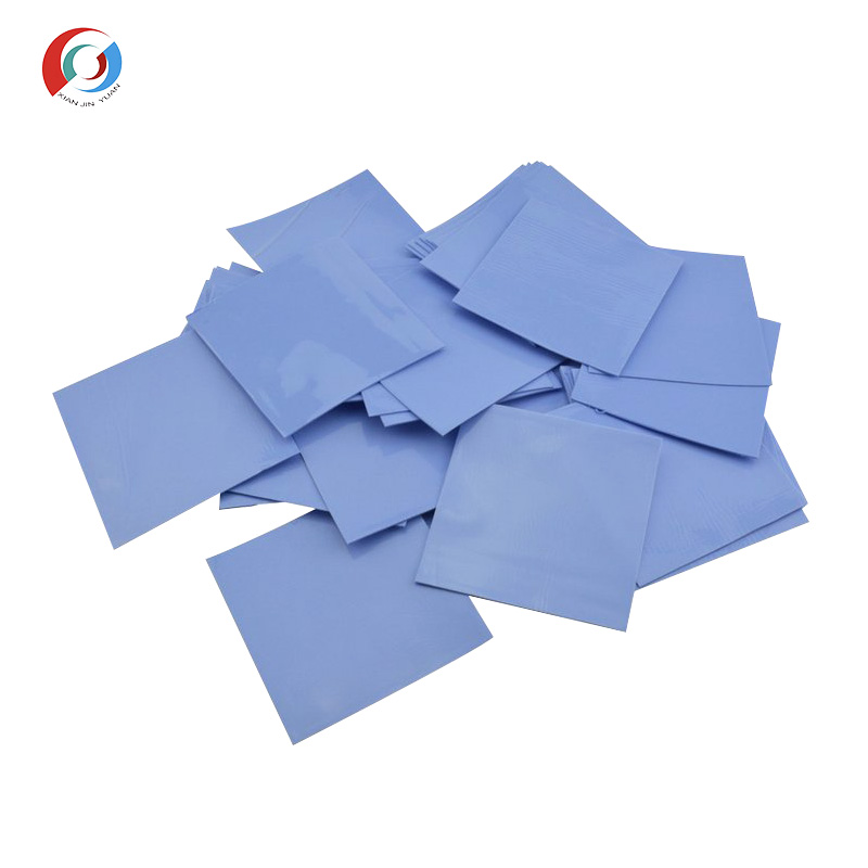
2、 Dual functional synergy: how thermal conductivity and absorption coexist in the same material
Thermal conductivity and absorption coexist in the same material system, and there is a natural contradiction in materials science. Thermal conductivity requires filling high thermal conductivity fillers (such as alumina, boron nitride, aluminum nitride, etc.) in the polymer matrix and forming a continuous thermal conductivity network; Absorbing requires filling with absorbers with electromagnetic loss capability (such as soft magnetic alloy powder, ferrite, carbon materials, etc.). The dispersion, orientation, and interface state of two types of fillers in the matrix directly affect the efficiency of achieving two functions.
The non silicon thermal conductive absorbing wave plate of Advanced Institute Technology has found the optimal balance between two functions through precise composite formula design and filler compounding technology. Its technical logic can be summarized into three levels.
The combination of fillers is the foundation for achieving dual functionality. By compounding thermal conductive fillers (such as nanoscale alumina) with absorbers (such as sheet-like soft magnetic alloy powder) in a specific ratio and particle size distribution, a composite network is constructed in a non silicon polymer matrix that combines thermal conductivity and electromagnetic loss pathways. Research has shown that by using directional assembly technology and polymer matrix composite, the dual effects of thermal conductivity and absorption can be achieved in the same material.
The microstructure design determines the upper limit of performance. The orientation and arrangement of thermal conductive fillers affect the directionality of thermal conductivity, while the dispersion state of absorbers affects the frequency response of electromagnetic parameters. Advanced Institute Technology has achieved synergistic optimization of thermal conductivity and absorption performance by regulating the diameter to thickness ratio, filling ratio, and dispersion process of fillers. Some products have a longitudinal thermal conductivity of over 5W/m · K, while maintaining an electromagnetic wave absorption rate of over 0.8.
Impedance matching is the "ticket" to the absorption efficiency. Non silicon thermal conductive absorbing wave plates are designed with gradient impedance matching, allowing electromagnetic waves to "enter" the interior of the material instead of being reflected on the surface, thereby achieving effective absorption. The absorption frequency band can cover a wide frequency range of 6-40GHz.
The non silicone polymer matrix itself also provides excellent temperature resistance and reliability. Through innovative molecular cross-linking technology, the material maintains stable dielectric properties at temperatures ranging from -40 ℃ to 200 ℃, solving the industry pain point of traditional silicon-based materials that are prone to high-temperature aging.
3、 Three core application scenarios: When "silicon free" and "dual functionality" become dual essential needs
Aerospace and satellite electronics are the application fields that require the highest reliability for non silicon thermal absorbing wave plates. The space of the aerospace electronic equipment cabin is extremely limited, but it needs to accommodate radar modules, communication payloads, and power conversion units simultaneously. High power density operation generates a large amount of heat, while close installation between high-frequency modules poses serious electromagnetic interference risks. The traditional approach adopts a layered arrangement of independent thermal management materials and electromagnetic shielding materials, which often increases system weight and assembly complexity. Non silicon thermal absorbing wave plates solve the two major problems of heat dissipation and EMI suppression simultaneously with a single material. Its non silicon properties are particularly important in vacuum environments - volatile substances of low molecular weight siloxanes may condense on low-temperature surfaces, contaminating optical devices or sensitive circuits. In addition, the material must pass low gas emission testing requirements such as ASTM E595. In aviation electronic equipment cabins, satellite communication modules, radar systems, and other scenarios, non silicon thermal absorbing wave plates are becoming the preferred solution that combines lightweight and high reliability.
5G/6G communication and optical modules are one of the areas with the highest demand for non silicon thermal absorbing wave plates. In 5G base stations and optical communication equipment, components such as power amplifiers, RF front-end modules, and optical modules face dual challenges of high heat generation and high-frequency electromagnetic interference. Thermal absorbing wave plates can be used in scenarios such as base station power amplifiers and optical modules, while solving high-frequency signal interference and heat dissipation problems. In optical modules, the value of non silicon properties is particularly prominent - the cleanliness of the lens surface directly determines the quality of the optical path, and any siloxane contamination may cause signal attenuation. As the electricity demand for data centers is expected to increase to approximately 945 TWh by 2030, the collaborative demand for thermal management and electromagnetic compatibility materials in AI computing infrastructure will continue to amplify.
New energy vehicles and intelligent driving represent the fastest-growing application directions. Vehicle mounted millimeter wave radar (24GHz, 77GHz and other frequency bands), laser radar, electronic control unit (ECU), battery management system (BMS) and other components require efficient heat dissipation to ensure stable operation of power devices, as well as suppression of electromagnetic interference to prevent sensitive signals from being contaminated. The procurement volume of millimeter wave radar absorbing materials for vehicles in 2025 will increase by 22% year-on-year. Non silicon thermal absorbing wave plates can be used inside vehicle radar modules to suppress cavity resonance, reduce sidelobe interference, and conduct heat to the heat dissipation structure. In autonomous driving sensors and controllers, non silicon thermal absorbing plates help improve the reliability of the system in complex electromagnetic environments. In addition, non silicon properties avoid the potential contamination risk of silicone oil precipitation on PCB board contacts, which is particularly critical for long-term automotive electronics.
4、 Selection points and design suggestions
Engineers need to focus on the following dimensions when selecting non silicon thermal absorbers: thermal conductivity and thermal resistance - the required thermal conductivity is evaluated based on chip power consumption and heat sink performance. Different power density devices have significant differences in thermal conductivity requirements; Absorption frequency band matching - The optimal absorption frequency band for different material systems varies, and it needs to be matched according to the main interference frequency of the equipment (from MHz to millimeter wave); Thickness and installation space - Non silicon thermal absorbing wave plates can be as thin as 0.2mm, suitable for space limited scenarios; Environmental tolerance - requires evaluation of operating temperature range (-40 ℃ to 200 ℃), flame retardant rating (such as UL94 V-0), and low gas release requirements (such as ASTM E595).
Advanced Institute Technology provides full process technical support from material selection, performance testing to sample trial production and batch delivery, helping customers incorporate non silicon thermal conduction and absorption solutions into system considerations in the early stages of product design.
5、 Outlook
The global market for thermal absorbing wave plates is in a high-speed growth channel. At the same time, the absorbing material industry is fully penetrating from a single military use to high-end civilian manufacturing. Driven by the construction of 5G/6G communication infrastructure, the deep evolution of automotive intelligence and electrification, the continuous upgrading of aerospace equipment, and the accelerated expansion of AI computing infrastructure, non silicon thermal absorbing plates that combine thermal conductivity and absorption functions and do not contain silicon components are moving from "professional material selection" to standard configurations for high reliability electronic equipment thermal management and electromagnetic compatibility design.
At the same time, the industry is continuously evolving towards the direction of "thinning, flexibility, broadband, and integration". The research and development of integrated materials for thermal conductivity and absorption is shifting from "simple blending" to "structural design" - cutting-edge technologies such as biomimetic 3D network structures and heterogeneous interface engineering are constantly expanding the performance boundaries of this material. Advanced Institute (Shenzhen) Technology Co., Ltd. will continue to deepen its cultivation in the field of non silicon functional composite materials, providing customers with higher performance and more reliable integrated thermal management and electromagnetic compatibility solutions through material innovation and process optimization.
 en
en  Español
 Français
 Português



