In the modern electronic information industry, printed circuit boards (PCBs) serve as the "skeleton" of electronic components, and their performance directly determines the reliability and integration of terminal equipment. With the rapid development of technologies such as 5G communication, artificial intelligence, and the Internet of Things, high-frequency, high-speed, and high-density interconnection have become the core development direction of PCBs. As a key technology for achieving interlayer conductivity in multi-layer boards, through-hole technology has attracted much attention for its material and process innovation. Among them, PCB through-hole copper paste has gradually become one of the core materials in high-end PCB manufacturing due to its excellent conductivity, reliability, and process adaptability.
1PCB through-hole copper pasteCore Value: From Material Characteristics to Technological Advantages
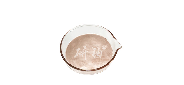
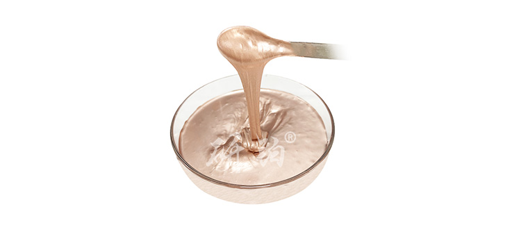
PCB through-hole copper paste is a conductive paste designed specifically for the through-hole process of printed circuit boards. It is mainly composed of high-purity copper powder, resin matrix, and special additives mixed together. Its core function is to form stable electrical connections by filling the conductive holes of the PCB board, while improving the mechanical strength and signal transmission efficiency of the circuit board.
1. Material characteristics: Dual guarantee of conductivity and stability
High quality through-hole copper paste needs to have three core characteristics:
High conductivity: The copper powder content is high and evenly dispersed, ensuring extremely low electrical resistivity of the conductive layer and meeting the signal transmission requirements of high-frequency circuits. For example, by optimizing the particle size and ratio of copper powder, the research platinum brand through-hole copper paste can achieve conductivity with a resistance as low as 2 milliohms. Heat and corrosion resistance: able to adapt to high-temperature curing processes in PCB manufacturing (such as 80-100 ℃ oven curing), and maintain stable performance in complex environments, avoiding conduction failure caused by oxidation or corrosion. Good process adaptability: It has excellent fluidity and thixotropy, suitable for various processes such as screen printing and spraying, and can accurately fill conductive holes of different apertures, especially suitable for complex structures such as multi-layer boards and high-density interconnects (HDI).
2. Technological advantage: Breaking through the bottleneck of traditional craftsmanship
Compared to traditional through-hole techniques such as chemical copper deposition and electroplating, the copper paste through-hole process has significant advantages:
Lower cost: No need for expensive electroplating equipment, high material utilization, can reduce PCB manufacturing costs by more than 30%.
Higher efficiency: Simplified process flow (such as screen printing high-temperature curing), reduced production cycle by 50%, suitable for large-scale production.
Better environmental protection: No "three wastes" emissions, compliant with environmental standards such as RoHS, reducing the cost of environmental treatment for enterprises.
Wide adaptability: Suitable for various substrates such as rigid boards, flexible boards (FPC), and rigid flexible composite boards, meeting the needs of multiple fields such as consumer electronics, automotive electronics, aerospace, etc.
IIAdvanced Institute of TechnologyLeading the innovation and application of through-hole copper paste technology
In the field of PCB through-hole copper paste, Advanced Institute (Shenzhen) Technology Co., Ltd. (hereinafter referred to as "Advanced Institute Technology") has become a leading material solution provider in the industry with years of technical accumulation and R&D investment. The company focuses on innovation in electronic materials, and its independently developed through-hole copper paste series products have "high efficiency, high reliability, and process friendliness" as their core competitiveness. They are widely used in high-end fields such as high-frequency circuits, multilayer boards, and flexible electronics.
1. Technological breakthrough: from material formulation to process optimization
Advanced Institute Technology's through-hole copper paste products have achieved key breakthroughs in the following areas:
Preparation of high-purity copper powder: Using nanoscale copper powder and special coating technology to enhance the dispersibility and antioxidant capacity of copper paste, ensuring long-term conductivity stability. Environmentally friendly resin system: Develop solvent-free, low VOC resin matrix to reduce environmental pollution during production, while enhancing the adhesion between copper paste and PCB substrate (shear strength can reach over 45MPa). Rapid curing process: By using flash sintering technology, the curing time is shortened to one-third of traditional processes, greatly improving production efficiency. For example, its "flashing lamp sintered copper paste" can be cured in a few seconds, making it suitable for consumer electronics production lines with extremely high production capacity requirements.
2. Application scenario: Covering the entire electronic manufacturing chain
Advanced Institute of TechnologyHigh reliability PCB copper pasteWidely serving the electronic manufacturing industry chain, typical applications include:
High frequency communication equipment, such as 5G base station antennas and routers, can reduce signal transmission attenuation and improve device communication speed due to the low loss characteristics of copper paste. Multi layer high-density PCB: By accurately filling blind holes and buried holes, interlayer interconnection is achieved, supporting high-end products such as chip level packaging (SiP) and IC carrier boards. Flexible electronic devices: Developed flexible copper paste to meet the bending requirements of FPC, ensuring conductivity even after repeated bending, suitable for wearable devices, foldable phones, etc.
3. Customer Value: Cost Reduction, Efficiency Enhancement, and Quality Improvement
Through technological innovation, Advanced Institute Technology's through-hole copper paste creates multiple values for customers:
Reduce production costs: Material prices are 15% -20% lower than imported products, and the process adaptability is strong, reducing equipment investment.
Improve product yield: Copper paste filling has high uniformity, with a penetration rate of over 99.5%, reducing the risk of scrap caused by poor hole filling.
Customized service: Adjust parameters such as copper paste viscosity and curing conditions according to customer needs, and provide an integrated solution from materials to processes.
3、 Industry trend: Future development direction of through-hole copper paste
With the development of electronic devices towards "smaller, faster, and more reliable", PCB through-hole copper paste will usher in three major development trends:
Refinement and miniaturization: In response to the demand for micro conductive holes (aperture<0.1mm) in HDI boards, we have developed ultrafine copper powder (particle size<1 μ m) copper paste to improve filling accuracy.
Multi functional integration: Integrating functions such as thermal conductivity and shielding, developing an integrated copper paste for "conductive heat dissipation" to meet the thermal management needs of high-power devices.
Deepening green manufacturing: promoting the research and development of lead-free and cadmium free copper paste, responding to global environmental regulations, and helping the sustainable development of the electronics industry.
Conclusion
Lead free environmentally friendly PCB copper pasteAs the "neural network" of electronic interconnection, its technological level is directly related to the innovation height of the electronic information industry. Advanced Institute Technology and other enterprises are continuously breaking through industry bottlenecks through material innovation and process optimization, providing more efficient and reliable solutions for high-end PCB manufacturing. In the future, with the deepening application of technologies such as 5G and AIoT, through-hole copper paste will play a more critical role in the field of electronic manufacturing, promoting "Chinese intelligent manufacturing" to move towards the high-end of the global value chain.

 en
en  Español
 Français
 Português



