Polyether ether ketone (PEEK), as a semi crystalline thermoplastic special engineering plastic, has been widely used in aerospace, electronic and electrical, medical equipment, and new energy fields due to its excellent high temperature resistance, mechanical strength, chemical stability, and electrical insulation properties. PEEK film can operate stably in environments above 250 ° C for a long time, with a stable dielectric constant of around 3.2 and a dielectric loss tangent value as low as 0.0015 in the 1-10 GHz frequency band, making it an ideal dielectric material for high-frequency signal transmission scenarios.
However, the inherent insulation and surface inertness of PEEK film pose technical bottlenecks in applications that require conductivity, electromagnetic shielding, or signal transmission functions. How to achieve reliable surface metallization without compromising the performance of PEEK film is an important issue in the field of material processing.
1、 Core performance advantages of PEEK film
The comprehensive performance of PEEK film is in a leading position in engineering plastics. Its continuous use temperature can reach 250 ° C, and its short-term heat resistance can exceed 300 ° C. It can still maintain dimensional stability and mechanical properties in high temperature environments. In terms of electrical performance, the dielectric constant of PEEK film at a frequency of 1 MHz is about 3.2-3.3, and the dielectric loss factor is about 0.003-0.005; In the 20 GHz frequency band, the dielectric loss can be as low as around 0.0035, which can significantly reduce the delay and energy loss in high-frequency signal transmission. At the same time, PEEK film has high breakdown voltage, low water absorption rate, and excellent radiation resistance, which can adapt to the complex working conditions inside spacecraft and aircraft engines. In addition, PEEK film has good biocompatibility and its elastic modulus is similar to that of human bones, making it uniquely advantageous in the field of medical implants.
2、 The core challenge of metalization
PEEK film itself is an excellent insulating material with low surface energy, high crystallinity, and strong chemical inertness, making it difficult for metal coatings to directly adhere. The biological inertness of PEEK is its main weakness as an implant material - it cannot directly bond with bones and lacks bone integration ability. Therefore, PEEK films must undergo surface activation treatment before undergoing various metallization processes such as chemical plating or physical vapor deposition (PVD).
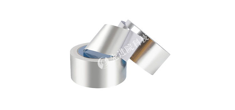
3、 The technological path of metallization
The surface metallization process of PEEK film usually includes three key steps: surface activation pretreatment, establishment of conductive layer, and deposition of functional layer.
(1) Surface activation: the primary step determining the success or failure of metallization
The activation methods currently used in the industry mainly include chemical roughening and plasma treatment. Chemical roughening uses chromic acid sulfuric acid system or potassium permanganate system to etch micro pits on the surface of PEEK, while introducing polar groups to enhance surface energy. Plasma treatment generates active sites on the surface of thin films through gas discharge, effectively improving the adhesion of metal coatings.
Advanced Institute (Shenzhen) Technology Co., LtdIn process practice, it has been found that plasma activation combined with low-energy ion beam pretreatment can effectively shorten the induction time of subsequent chemical plating, and has a smaller impact on the mechanical properties of the film itself. This combination scheme has obtained stable binding force data in sample validation.
(2) Chemical plating: standard scheme for establishing conductive layer
After completing surface activation, a conductive layer needs to be established on the surface of PEEK. Chemical plating is the most widely used solution, among which electroless nickel plating (Ni-P alloy) is considered the standard process due to its mature technology and uniform coating. The electroless nickel plating layer not only endows PEEK film with conductivity, but also serves as a bottom layer for subsequent electroplating. National StandardGB/T 43763-2024 "Aerospace functional coatings - Special non-metallic materials - Metal coatings"It has been clearly stipulated that various metal coatings such as nickel gold, nickel silver, copper nickel gold, etc. can be prepared on the surface of special non-metallic materials such as PEEK using electroplating or chemical plating methods.
On this basis, the following metals can be electroplated according to specific functional requirements:
- Copper (Cu)Enhance conductivity and heat dissipation performance
- Gold (Au): Used for high-frequency signal transmission
- Silver (Ag)Enhance electromagnetic shielding effect
(3) Physical Vapor Deposition (PVD): The Optimal Route for Ultra Thin Low Temperature Coatings
PVD processes such as magnetron sputtering and vacuum evaporation can deposit metal thin films at low temperatures, with film thickness typically controlled within the range of 50-500 nanometers, which can avoid high-temperature damage to the semi crystalline structure of PEEK. PVD sedimentable metals include:
- Titanium (Ti): Used for medical bone integration
- Chromium (Cr)Used for wear-resistant coatings and adhesion promoting layers
- Gold/Silver/Aluminum (Au/Ag/Al)Used in decoration, microelectronics and other fields
(4) Cutting edge technology
- Femtosecond laser modification assisted chemical platingWe have achieved the production of highly conductive and strongly bonded metal copper patterns on localized areas of PEEK surfaces, providing a new approach for the production of functionalized metal patterns on polymer surfaces for aerospace applications.
- Hybrid additive manufacturingBy combining fused deposition modeling (FDM) with laser activated metallization (LAM) technology, micro nano composite structures and chemically active groups can be introduced onto the surface of PEEK, forming a PEEK Cu interface that combines mechanical interlocking and chemical bonding.
4、 Typical application scenarios
(1) Medical implants: from bioinertness to active osseointegration
PEEK is widely used in fields such as spinal fusion devices, and its elastic modulus is extremely close to that of human bones. However, its biological inertness limits its bone integration ability. Through surface metallization modification, this bottleneck is being overcome:
- Titanium or Strontium Titanate (STO) CoatingBy using magnetron sputtering technology to deposit titanium or strontium titanate films on the surface of PEEK, the osteogenic effect can be significantly enhanced.
- Tantalum (Ta) ion implantationAdding tantalum to the surface of PEEK can promote the generation of osteoblasts and enhance bone integration.
- composite coatingPreparing a composite coating containing cerium silver zinc oxide on the surface of PEEK can improve the material's biocompatibility, osteogenic properties, and antibacterial properties.
The metalized PEEK implant achieves better bone integration performance while maintaining an elastic modulus similar to that of human bones, providing a better solution for the field of orthopedic implants.
(2) High frequency electronics and 5G communication: key materials for low loss signal transmission
PEEK is mainly used as a low loss, high reliability substrate and antenna material in 5G communication, helping to achieve efficient transmission of high-frequency signals, miniaturization of equipment, and long-term operational stability. PEEK film is widely used in the fields of flexible circuit boards (FPC), insulation gaskets, and high-frequency motors, which can effectively reduce signal loss and improve the electrical safety and energy efficiency ratio of system operation.
The metalized PEEK film further expands its application boundaries:
- 5G communication substrate and antennaCopper or gold plated PEEK film can be used for 5G communication substrates, antennas, and flexible circuits, and its low dielectric loss characteristics help reduce high-frequency signal transmission delay.
- Femtosecond laser modification assisted chemical platingHigh precision metal patterning can be achieved on the surface of PEEK, providing a new path for high-precision manufacturing of high-frequency circuits.
(3) Electromagnetic shielding and aerospace
PEEK based composite materials have been widely used as alternative materials to metals for electromagnetic shielding. Metallized PEEK film provides excellent electromagnetic shielding performance while maintaining its lightweight advantage, and is widely used in the fields of communication electronics and aerospace. Nickel/copper plated PEEK film can be used as an electromagnetic shielding material to replace traditional metal components, achieving lightweight while meeting electromagnetic compatibility requirements.
5、 Technology Outlook and Company Advantages
The metallization technology of PEEK film still faces dual challenges of cost and process complexity. However, multiple technological advancements are driving this field forward: the improvement of plasma activation efficiency, the development of environmentally friendly roughening solutions, the maturity of femtosecond laser modification technology, and the decrease in PVD equipment costs are driving the expansion of metalized PEEK films into a wider range of application areas.
Advanced Institute (Shenzhen) Technology Co., LtdEstablished in 2016, located in Bao'an District, Shenzhen, it is a national high-tech enterprise focusing on shielding materials, insulation materials, thermal conductivity materials, and precious metal coatings. The company has the following core advantages in the field of PEEK film metallization:
- Technical Roadmap: Covering chemical plating PVD、 Various metallization processes such as ion implantation
- Coating systemNickel, copper, gold, silver, titanium, chromium and their alloys
- Process guaranteeBy establishing an orthogonal process window for plasma treatment power, gas pressure, and coating peeling strength, ensure stable inter batch bonding force
- Application SupportCustomized metallization solutions can be provided according to customer needs, covering multiple fields such as medical implants, high-frequency electronics, electromagnetic shielding, etc
With the continuous development of industries such as 5G/6G communication, aerospace lightweighting, and biomedicine, PEEK film metallization technology is expected to maintain a steady growth trend.Advanced Institute (Shenzhen) Technology Co., LtdWe will continue to delve into the field of PEEK film metallization and provide customers with highly reliable and consistent technical solutions.
Contact Us
Advanced Institute (Shenzhen) Technology Co., Ltd
Customized Hotline:0755-22277778
mobile phone13826586185 (Mr. Duan)
Fax0755-22277776
Email:duanlian@xianjinyuan.cn
Address:8th Floor, Zhongxing Building, Xinsha Road, Shajing, Bao'an District, Shenzhen, Guangdong Province, China
Official website:www.xianjinyuan.cn
*Welcome to inquire by phone for more product information or customized solutions.
*This article is compiled by the technical team of Advanced Institute (Shenzhen) Technology Co., Ltd., aiming to provide professional reference for PEEK film metallization technology for customers and industry partners.
 en
en  Español
 Français
 Português



