Introduction
In the current era of rapid technological development, new materials continue to emerge, bringing innovative changes to many fields. Advanced Institute of Technology's research and development, production, and salesPI copper plated filmWith its unique craftsmanship and outstanding performance, it has become a shining star in the field of materials, attracting the attention of many research institutions and enterprises. Lanzhou Institute of Physics is one of them.
Vacuum Sputtering: The Exquisite Manufacturing Password of PI Copper Coating
The birth of PI copper plated film cannot be separated from advanced vacuum sputtering technology. In a highly clean vacuum environment, a wonderful reaction of the microscopic world quietly unfolds. High speed particles, like precise "shells," bombard the surface of copper targets. Under the impact of strong energy, atoms or molecules on the surface of copper target are excited, breaking free from their original constraints and splashing around at extremely high speeds. These splashing copper atoms or molecules are directionally deposited on the surface of PI thin films under the clever guidance of electric and magnetic fields.
This process is like a skilled craftsman meticulously carving a piece of art. After continuous and stable deposition, a uniform and dense copper film gradually forms on the surface of the PI film. This unique manufacturing method endows PI copper plated film with many advantages. The uniform coating ensures the consistency of material performance in different areas, demonstrating stable and reliable performance in both electronic transmission and thermal conduction. The strong adhesion enables the copper film to tightly bond with the PI film, as if they were one body. In the subsequent use process, it is not easy to have problems such as detachment and delamination, greatly extending the service life of the material. At the same time, the entire vacuum sputtering process has minimal impact on the original properties of PI films, allowing them to maintain excellent characteristics such as flexibility and insulation, providing broad space for subsequent processing and applications.
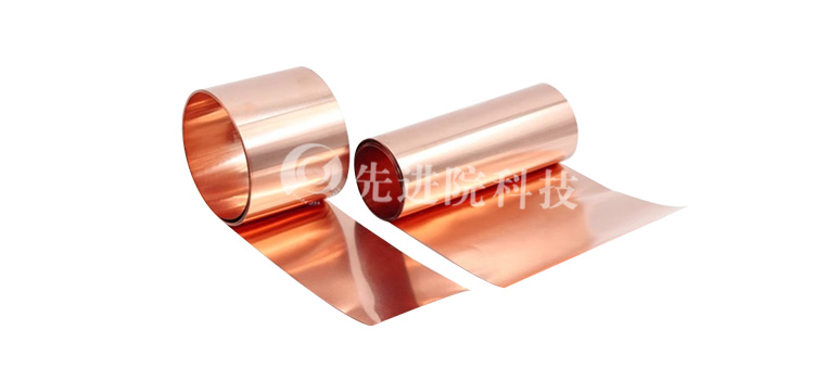
Thickness customization: a flexible choice to meet diverse needs
Advanced Institute of TechnologyWe are well aware that different application scenarios have differentiated requirements for material thickness, thus providing a rich and diverse range of thickness choices for PI copper plated films. From thin and light options of 5 μ m to thick materials of 125 μ m, it covers a wide range of thicknesses. This rich thickness specification is not simply a numerical variation, but a precise adaptation for different industries and products.
In some fields with high requirements for lightweight materials, such as flexible electronic devices, thin PI copper plated films with a thickness of 5-20 μ m can fully leverage their advantages. It can ensure good conductivity while minimizing device weight, achieving lightweight and portability, and providing users with a more comfortable user experience. In some scenarios that require high strength and conductivity, such as electromagnetic shielding, battery electrodes, etc., a thick PI copper plating film of 80-125 μ m can demonstrate strong strength. Its thick copper film layer can provide a more stable and efficient conductive path, effectively meeting the working requirements of high power and high load. More thoughtfully, Advanced Institute Technology also supports customized thickness as needed. Customers can communicate with the professional team of Advanced Institute Technology to determine the most suitable thickness specification based on their own product requirements, truly achieving personalized customization services.
Scientific research recognition: The selection of a physics institute in Lanzhou bears witness to its quality
Lanzhou Institute of Physics, as a leader in the field of domestic scientific research, has a profound accumulation and strict screening standards in material research and application. After multiple rounds of rigorous testing and evaluation, the institute ultimately chose to purchase PI copper plated film from Advanced Institute, which undoubtedly highly recognizes the quality of Advanced Institute's technological products.
In the research project of a certain physics institute in Lanzhou, PI copper plating film provided strong support for the smooth implementation of the experiment due to its excellent performance. Its uniform coating and good adhesion ensure the accuracy and stability of experimental data; Rich thickness specifications meet the diverse needs of different experimental scenarios. This cooperation case not only demonstrates the strong competitiveness of advanced institute technology PI copper plating film in the field of scientific research, but also provides a powerful reference for more research institutions and enterprises to choose this product.
PI copper plated filmWith its advanced vacuum sputtering manufacturing process, flexible thickness customization services, and excellent quality recognized by scientific research institutions, it has occupied a place in the materials field. With the continuous advancement of technology, we believe that PI copper plated film will shine in more fields and contribute important strength to promoting industry development.

 en
en  Español
 Français
 Português



