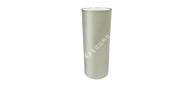
In the current era of rapid development of electronic technology, the research and application of high-performance materials have become a key driving force for industry progress.Nickel plating on PI filmAs a leader among them, technology has shown tremendous potential for applications in various fields such as communication and electronics, thanks to its unique performance advantages. Advanced Institute Technology has been deeply involved in this field, and its PI thin film nickel plating products have won widespread recognition in the market with exquisite craftsmanship and excellent quality. The procurement of a well-known communication company in Shenzhen is a strong example.
PI film: the cornerstone of nickel plating process
PI film, also known as polyimide film, is a high-performance organic polymer material. It has excellent high temperature resistance and can maintain stable physical and chemical properties over a wide temperature range. It can handle both long-term work in high-temperature environments and applications under extremely low temperature conditions with ease. At the same time, PI film also has excellent insulation performance, mechanical properties, and chemical corrosion resistance, which make it an ideal substrate for many high-end electronic products.
The preparation of PI film is crucial in the nickel plating process of PI film. Advanced Institute Technology strictly controls the quality of raw materials and selects high-quality PI films to ensure uniform thickness and smooth surface, laying a solid foundation for subsequent nickel plating processes. Precision cutting of PI film to meet the customized needs of different customers, whether it is a specific size of film or a special shape of product, can be delivered accurately.
Surface pretreatment: Open the door to nickel plating
The PI film itself does not have conductivity, which poses certain challenges to the nickel plating process. The surface pretreatment process is the key step in solving this problem.Advanced Institute of TechnologyUsing advanced processing techniques, clean and roughen the surface of PI film. The cleaning process can remove impurities and pollutants from the surface of the film, ensuring the adhesion of the coating; Coarsening treatment is achieved through physical or chemical methods to form a micro rough structure on the surface of the film, increase the surface area, and enhance the bonding strength between the nickel layer and the PI film.
After surface pretreatment, the PI film surface has good activity, creating favorable conditions for subsequent chemical plating or electroplating of nickel layers. This step is like building a solid framework for a building, only when the framework is built firmly can the subsequent construction proceed smoothly.
Chemical plating and electroplating: the magnificent appearance of nickel layer
Chemical nickel plating and electroplating nickel plating are the two main ways to form a nickel layer. Chemical nickel plating forms a uniform nickel layer on the surface of PI film through self catalytic reaction. In a specific chemical solution, nickel ions are reduced to metallic nickel on the surface of PI thin films with catalytic activity, and continuously deposited, gradually forming a dense and uniform nickel layer. The advantage of this method is that it does not require external current and can achieve uniform coating on complex shaped thin film surfaces, with stable coating performance.
Electroplating nickel requires a conductive substrate or a pre deposited conductive seed layer through methods such as sputtering. Under the action of an electric field, nickel ions move towards the cathode (i.e. the surface of the PI film) and reduce and deposit on the conductive seed layer, forming a nickel layer. Electroplated nickel plating can achieve thicker coatings with higher hardness and good wear resistance. Advanced Institute Technology flexibly selects chemical plating or electroplating processes according to customers' different needs, and provides customized solutions for customers.
Post processing: sublimation of quality
After nickel plating is completed, the post-treatment process is indispensable. Advanced Institute Technology performs cleaning, drying, and other operations on the nickel plated PI film to remove residual chemical substances on the surface and prevent corrosion to the coating and film. Perform performance testing on the coating, such as thickness measurement, adhesion testing, corrosion resistance testing, etc., to ensure that each PI thin film nickel plated product meets high quality requirements.
A well-known communication company in Shenzhen has purchased Advanced Institute'sNickel plating on PI filmThe product is precisely based on its advanced technology and reliable quality. The application of PI thin film nickel plating technology in the field of communication can effectively improve the performance and reliability of electronic components, providing strong support for the miniaturization and high performance of communication equipment. With the continuous advancement of technology, PI thin film nickel plating technology is bound to usher in broader development prospects, injecting new vitality into the development of the electronics industry.

 en
en  Español
 Français
 Português



