Polydimethylsiloxane (PDMS), as an excellent organic silicone elastomer, occupies an important position in the fields of flexible electronics, microfluidic chips, wearable devices, and biomedical engineering due to its outstanding optical transparency, biocompatibility, and mechanical flexibility. However, the inherent hydrophobicity and chemical inertness of PDMS surface make it difficult for metal thin films to achieve firm adhesion on its surface, which has become a core technical bottleneck restricting the reliability and functional expansion of related devices.Advanced Institute (Shenzhen) Technology Co., LtdWe have been deeply involved in the field of flexible substrate coating for many years, and have developed a full chain process solution from surface pretreatment to metal deposition around PDMS substrate metallization, providing professional technical support and customized services for diverse application scenarios.
1、 PDMS material properties and metallization challenges
PDMS is composed of a silicon oxygen (Si-O) main chain and hydrophobic methyl side groups, with a glass transition temperature as low as about -120 ° C, endowing the material with stable high elasticity over a wide temperature range. By adjusting the ratio of prepolymer to curing agent (10:1 to 30:1) and curing temperature (room temperature to 150 ° C), the Young's modulus can be precisely adjusted within the range of 0.34 to 2.97 MPa. The visible light transmittance (400-800 nm) is higher than 90%, and the refractive index is about 1.41-1.43. However, the PDMS surface exhibits intrinsic hydrophobicity due to the dense arrangement of methyl groups, with a water contact angle of 100 ° -110 ° and a surface energy of only 19-22 mN/m. In addition, the chemical inertness is significant, making it difficult for metal atoms to establish effective chemical bonds with the surface. Directly using thermal evaporation or sputtering to deposit metal layers not only has extremely low adhesion and is prone to peeling, but also when the substrate temperature exceeds 150 ° C, residual oligomers or dissolved gases inside PDMS may escape, which may cause film foaming and local changes in the cross-linked network. This is a technical difficulty that needs to be addressed in flexible metallization processes.
2、 Surface pretreatment: a key step in breaking through the bottleneck of metal adhesion
To achieve a strong bond between metal and PDMS, surface activation treatment and interface engineering optimization must be carried out. Advanced Institute Technology adopts plasma pretreatment technology, which effectively improves the bonding strength between the substrate and the metal layer by bombarding the substrate surface with plasma. Oxygen plasma treatment (power 50-200 W, oxygen flow rate 20-50 sccm, time 30-120 seconds) can oxidize the surface hydrophobic silicon methyl group (Si CH3) to hydrophilic silanol (Si OH) groups, reducing the water contact angle from about 110 ° to below 5 ° and increasing the surface energy to 30-70 mN/m, providing dense polar binding sites for metal nucleation. It should be noted that the plasma activation effect gradually deteriorates within about 1 hour in air (i.e., the "aging" phenomenon), so metal deposition should be completed as soon as possible after treatment. To further enhance the reliability of the interface, self-assembled monolayers (such as APTES, MPTS) can be introduced on the activated surface, and amino or thiol functional groups can be grafted to enhance the chemical affinity with metals such as gold and silver; Alternatively, chromium (Cr) or titanium (Ti) with a thickness of 5-20 nm can be pre sputtered as an adhesive layer. By utilizing physical interlocking and atomic interdiffusion effects, the interfacial peel strength can be increased to several N/cm levels, providing a stable substrate for subsequent functional metal layers.
3、 Gold (Au): the preferred conductor for flexible electrodes and biosensing
Gold has become the most widely used conductor material in PDMS metallization due to its excellent oxidation resistance, low electrical resistivity (2.44 × 10 ⁻Ω· m), and good biocompatibility. The deposition methods include thermal evaporation (source temperature of about 1000-1500 ° C, substrate water cooling to maintain room temperature) and magnetron sputtering (power density of 2-5 W/cm ², argon pressure of 0.5-2 Pa), and the film thickness can be controlled within the range of 10 nm to several hundred nanometers. After activation by oxygen plasma and optimization of the adhesion layer, the peel strength between the gold film and PDMS can exceed 2 N/cm, and the relative resistance change rate is controlled within 20% under 30% tensile strain. The chemical inertness of gold endows gold-plated electrodes with excellent corrosion resistance, making them suitable for long-term implantation scenarios. Flexible electrodes based on Au/PDMS have been widely used in epidermal EEG/ECG sensors, electrochemical immunosensing platforms (such as antibody molecule immobilization), and surface enhanced Raman scattering substrates - the latter can provide signal enhancement factors on the order of 10 ⁶, enabling highly sensitive detection of trace biomarkers.
4、 Silver (Ag): Integrated high conductivity transmission and antibacterial function
Silver has the lowest electrical resistivity among all metals (1.59 × 10 ⁻⁸Ω· m), making it an ideal material for building highly conductive flexible circuits and wireless RF antennas. When preparing silver films by magnetron sputtering, the film thickness should be controlled within 200 nm to avoid cracking under tension; By designing a micro scale corrugated structure with a cycle of 8 μ m, the stretchability can be significantly improved. Ultra thin silver layer (thickness less than 20 nm) can balance light transmittance (above 80%) and conductivity, making it suitable for transparent electrodes in wearable devices. Silver ions endow the film with natural broad-spectrum antibacterial properties, making it suitable for making surface electrodes for medical catheters or wound monitoring patches, achieving integrated functions of electrophysiological signal acquisition and bacterial infection protection. Advanced Institute Technology adopts nano silver wire composite technology in silver plating process to form a three-dimensional conductive network, further improving the conductivity performance.
5、 Aluminum (Al): Optical Reflective Layer and Electromagnetic Interference Shielding Layer
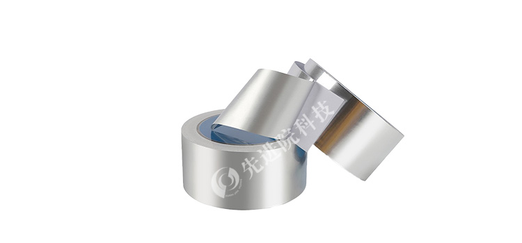
After aluminum is activated by oxygen plasma (with water contact angle reduced to below 10 ° C), it can be deposited on the surface of PDMS through thermal evaporation (melting point of about 660 ° C) or sputtering process, forming a firmly attached metal layer. Aluminum film has a reflectivity of over 90% in the visible to near-infrared range, making it an ideal choice for optical devices such as flexible display backlight reflectors and foldable micro mirror arrays. Meanwhile, with a resistivity of 2.65 × 10 Ω· m and cost advantages, aluminum also performs outstandingly in the field of electromagnetic compatibility: when the film thickness reaches 100 nm or more, the electromagnetic interference shielding effectiveness of the aluminum layer in the frequency range of 30 MHz to 1 GHz can reach 60 to 80 dB, providing reliable electromagnetic protection for wearable devices and flexible electronic packaging.
6、 Platinum (Pt) sensor electrode and Cr/Cu/Ni multilayer interconnect structure
Platinum (Pt) is mainly used in the field of electrochemical sensing (such as pH electrodes, glucose oxidase immobilization, etc.). Before deposition, a Cr or Ti adhesion layer (5-10 nm) must be introduced, followed by sputtering a Pt functional layer of 50-200 nm. After interface optimization, the bonding strength of Pt/PDMS can reach 4.412 MPa, and the impedance drift after 500 cycles of 80 ° bending is less than 18.3%, ensuring long-term sensing stability. The sintered resistivity of the platinum electrode slurry developed by Advanced Institute Technology is as low as 1.65 μ Ω· cm, and the square resistance is as low as 20 ± 5 m Ω/□, ensuring high sensitivity and fast response of the electrode. On the other hand, the chromium/copper/nickel (Cr/Cu/Ni) three-layer composite system is dedicated to microelectronic interconnects: the Cr layer (about 10 nm) ensures adhesion, the Cu layer (100-500 nm) serves as a low resistance conductive channel (resistivity 1.68 × 10 ⁻⁸Ω· m), and the Ni layer (50-100 nm) acts as a diffusion barrier to prevent copper oxidation. This combination can withstand repeated bending of flexible substrates and is widely used in high-density flexible circuit boards and internal wiring of MEMS devices.
7、 ITO transparent conductive film and low-temperature liquid metal substitution process
Indium tin oxide (ITO) is deposited on the surface of PDMS by radio frequency magnetron sputtering (substrate temperature controlled below 100 ° C, precise control of oxygen partial pressure), which can obtain a transparent conductive film with visible light transmittance higher than 90% and resistivity as low as ≤ 8 × 10 ⁻⁴Ω· cm. It is the preferred material for flexible touch screens and bendable LED electrodes. However, due to the low modulus characteristics of PDMS, ITO is prone to microcracks when uniaxial strain exceeds 15%, and it is necessary to use microstructure topology design (such as wavy geometry) or interface buffer layers to suppress crack propagation. It is worth noting that room temperature or low-temperature non vacuum processes are becoming an emerging alternative direction, such as inkjet printing of eutectic gallium indium (EGaIn) or gallium indium tin (GaInSn) liquid metal alloys, which can quickly construct flexible conductive patterns while avoiding thermal damage, broadening the process window for thermosensitive PDMS devices.
8、 Full chain process support and large-scale production capacity
Regardless of the metallization scheme used, the process chain of "surface activation → adhesion layer → functional layer deposition" must be strictly followed, and temperature parameters must be strictly controlled to avoid the risk of foaming caused by high temperatures. Advanced Institute Technology has independently built a magnetron sputtering and vacuum evaporation production line, which can continuously deposit metal layers on the surface of flexible polymer films. The process features include uniform coating, strong adhesion, and support for continuous roll to roll production, making it suitable for large-scale supply. Suitable substrates include various polymer materials such as FEP, PI, PET, LCP, PPS, PEN, PP, etc., and can be plated with metals including gold, silver, copper, aluminum, tin, nickel, titanium, platinum, etc. The company has passed the ISO9001 quality management system certification, and its products comply with the relevant military standards of GJB 773A and RoHS environmental requirements.
Advanced Institute (Shenzhen) Technology Co., Ltd. is deeply engaged in PDMS based flexible device metallization technology, providing full chain process support and customized solutions from surface pretreatment to metal deposition for fields such as flexible electronics, microfluidics, wearable sensors, biological interfaces, MEMS, and new energy.
Advanced Institute (Shenzhen) Technology Co., Ltd
Address: 8th Floor, Zhongxing Building, Xinsha Road, Xinqiao Street, Bao'an District, Shenzhen
Phone: 0755-222777778
Mobile: 13826586185 (Mr. Duan)
Email: duanlian@xianjinyuan.cn
URL:www.xianjinyuan.cn
(This article is based on industry general technical literature and company technical accumulation, for reference in technology selection and business negotiation)
 en
en  Español
 Français
 Português



