Polyether ether ketone (PEEK) is known as the "pyramid tip" of the special engineering plastics family. As a semi crystalline thermoplastic special engineering plastic, PEEK has been widely used in aerospace, electronic and electrical, medical equipment, and new energy fields due to its excellent high temperature resistance, mechanical strength, chemical stability, and electrical insulation properties.
PEEK film can operate stably in environments above 250 ° C for a long time, with a stable dielectric constant of around 3.2 and a dielectric loss tangent value as low as 0.0015 in the 1-10 GHz frequency band, making it an ideal dielectric material for high-frequency signal transmission scenarios. However, the inherent insulation and surface inertness of PEEK film pose technical bottlenecks in applications that require conductivity, electromagnetic shielding, or signal transmission functions.
1、 PEEK film gold plating: why has it become a necessity in the industry?
With the continuous increase in demand for high-performance materials in high-end fields such as 5G communication, aerospace, and medical equipment, the demand for metallization of PEEK films is becoming increasingly urgent. The global PEEK material market size has reached approximately 657 million US dollars by 2025, and is expected to exceed 1 billion US dollars by 2032. Among them, the global PEEK film market is expected to reach a sales volume of 1.217 billion yuan (approximately 179 million US dollars) in 2025, and is expected to grow to 1.844 billion yuan (approximately 271 million US dollars) in 2032, with a compound annual growth rate of 6.2%.
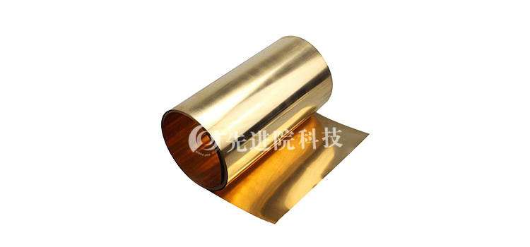
Among all metal coatings,gildingWith excellent conductivity, extremely low contact resistance, outstanding corrosion resistance, and biocompatibility, it has become the core technology path for functional upgrading of PEEK films. Gold plated PEEK film is widely used in high-end scenarios such as high-frequency signal transmission, aerospace connectors, 5G communication substrates, and medical implant devices.
2、 The technical challenge of gold plating on PEEK film
PEEK film itself is an excellent insulating material with low surface energy, high crystallinity, and strong chemical inertness, making it difficult for metal coatings to directly adhere. The biological inertness of PEEK is also one of its main weaknesses as an implant material - it cannot directly bond with bones and lacks bone integration ability. Therefore, PEEK film must undergo surface activation treatment before undergoing metalization processes such as chemical plating or physical vapor deposition.
The surface metallization of PEEK film usually involves three key steps:Surface activation pretreatment, establishment of conductive layer, and deposition of functional layerAny problem at any stage can lead to coating peeling or substandard performance.
3、 Advanced Institute Technology: Professional Manufacturer of PEEK Film Gold Plating
In the highly technical niche of PEEK coating, Advanced Institute (Shenzhen) Technology Co., Ltd. is a professional manufacturer worth paying attention to.
The company was founded in 2016 and is headquartered in Bao'an District, Shenzhen, Guangdong Province. It is a national high-tech enterprise focusing on shielding materials, insulation materials, thermal conductivity materials, and precious metal coatings. The company has its own registered trademark "Research Platinum" and has dual production bases in Shenzhen and Dongguan.
The company has passed.ISO9001 Quality Management System CertificationThe product complies withGJB 773A Aerospace Related StandardsandRoHS environmental requirementsCapable of supporting high-end fields such as aerospace, military, and 5G communication. National StandardGB/T 43763-2024 "Aerospace functional coatings - Special non-metallic materials - Metal coatings"It has been clearly stipulated that various metal coatings such as nickel gold coating, nickel silver coating, copper nickel gold coating, copper nickel silver coating, etc. can be prepared on the surface of special non-metallic materials such as PEEK using electroplating or chemical plating methods.
4、 Core process: Magnetron sputtering gold plating plasma activation
1. Magnetron sputtering coating technology
Advanced Institute of Technology has independently builtMagnetron sputtering and vacuum evaporation production line, usingContinuous production process of roll to rollIt can continuously and uniformly deposit metal layers on the surface of flexible polymer films. Suitable substrates include various flexible polymer films such as PEEK, PI, PET, LCP, FEP, PPS, etc., and can be plated with metals including gold, silver, copper, aluminum, tin, nickel, titanium, platinum, etc.
Magnetron sputtering is carried out in a vacuum environment, where high-speed particles bombard the target material, causing metal atoms to break free from the constraints of the target material and deposit uniformly on the surface of the thin film, forming a uniform and dense metal film. Compared with traditional chemical plating methods, PVD technology has the advantages ofEnvironmentally friendly, with good coating uniformity and strong adhesionBy leveraging these advantages, uniform deposition of metal atoms on the substrate surface can be achieved under low-temperature conditions.
Relying on advanced physical vapor deposition (PVD) technology, the thickness of metal thin films can be achievedNano level precise controlCustomized as needed within the range of a few nanometers to several hundred nanometers.
2. Plasma activation pretreatment
In response to the core challenges of low surface energy and strong chemical inertness of PEEK, Advanced Institute Technology has developedPlasma activation combined with low-energy ion beam pretreatmentworkmanship By bombarding the surface of the substrate with plasma, the bonding strength between the substrate and the metal layer is effectively improved. This combination scheme can effectively shorten the induction time of subsequent chemical plating, and has a smaller impact on the mechanical properties of the film body. Stable binding force data has been obtained in sample validation.
3. Electroplating thickening (optional)
For application scenarios that require thicker coatings, the metal layer can be further thickened through electroplating on the basis of magnetron sputtering. Metal coating passed throughGradient coating designRealize stress transition from the substrate to the metal layer, effectively avoiding interface delamination caused by modulus differences.
5、 Gold plating solution: precise matching of three major application scenarios
Advanced Institute Technology provides PEEK filmNickel plating, copper plating, gold plating, silver plating, titanium plating, chrome platingSix major plating schemes. among which,Gold plating schemeWith unique performance advantages, it plays an irreplaceable role in the following three high-end fields:
1. 5G communication applications
Gold plated PEEK film can be used for5G communication substrate, millimeter wave antenna, flexible circuitWaiting for high-frequency scenarios. The low dielectric loss characteristics of PEEK film (with a dielectric loss tangent value as low as 0.0015 in the 1-10 GHz frequency band) help reduce high-frequency signal transmission delay. The gold plating layer provides excellent conductivity and extremely low contact resistance, ensuring stable transmission of high-frequency signals. In the millimeter wave frequency band, the dielectric constant and loss of PEEK film are superior to traditional PI film.
2. Aerospace applications
Gold plated PEEK film withLightweight, heat-resistant, and excellent electromagnetic shielding performanceApplied to conductive structural components and signal transmission components inside spacecraft. Under the same conditions, PEEK pipes reduce weight by 65% compared to stainless steel pipes and 45% compared to titanium alloy pipes. Its radiation resistance can adapt to the complex working conditions inside spacecraft and aircraft engines. The release of the national standard GB/T 43763-2024 provides authoritative technical specifications for PEEK gold-plated products in the aerospace field.
3. Application of medical devices
Gold plated PEEK film can be used forImplantable electronic devices and artificial bone repair materialsPEEK material has good biocompatibility and radiation permeability. The gold coating has excellent biocompatibility and corrosion resistance, which can improve the surface activity of PEEK film and promote cell adhesion. The elastic modulus of PEEK is similar to that of human bones, and the gold plating layer can further enhance its comprehensive performance in medical implantation scenarios.
6、 Company qualifications and technological advantages
| Qualification/Technology |
Explanation |
| National high-tech enterprise |
Established in 2016, we specialize in shielding materials, insulation materials, thermal conductive materials, and precious metal coatings |
| ISO 9001 certification |
Quality management system certification ensures product quality stability |
| GJB 773A Aerospace Standard |
The product complies with aviation and aerospace related standards and has military supporting qualifications |
| GB/T 43763-2024 |
National standard for aerospace functional coating, PEEK gold plating has evidence to follow |
| Roll to roll magnetron sputtering |
Continuous production, uniform coating, suitable for bulk supply |
| Nano scale thickness control |
The thickness can be precisely customized within the range of a few nanometers to several hundred nanometers |
| Plasma activation |
Effectively improve the surface energy of PEEK and enhance the adhesion of the coating |
7、 Collaboration Contact
Advanced Institute (Shenzhen) Technology Co., Ltd. is committed to providing a one-stop solution for PEEK film gold plating in the high-end manufacturing field. We welcome new and old customers to contact us for consultation and negotiation.
- ChengAdvanced Institute (Shenzhen) Technology Co., Ltd
- Headquarters Address:8th Floor, Zhongxing Building, Xinsha Road, Shajing, Bao'an District, Shenzhen, Guangdong Province
- Customized Hotline:0755-22277778
- mobile phone13826586185 (Mr. Duan)
- Email:duanlian@xianjinyuan.cn
*The content of this article is for reference only. Please refer to the official information of the company for specific product parameters and quotations.
 en
en  Español
 Français
 Português



