Advanced Institute Technology PEEK film low-temperature titanium plating technology and roll to roll mass production plan
Low temperature gradient interface locking, width 600mm, film thickness as low as 6 μ m, roll to roll mass production
Overview
Polyether ether ketone (PEEK) is known as the "pyramid tip" of the special engineering plastics family. As a semi crystalline thermoplastic special engineering plastic, PEEK has been widely used in aerospace, electronic and electrical, medical equipment, and new energy fields due to its excellent high temperature resistance, mechanical strength, chemical stability, and electrical insulation properties. PEEK film can operate stably in environments above 250 ° C for a long time, with a stable dielectric constant of around 3.2 and a dielectric loss tangent value as low as 0.0015 in the 1-10 GHz frequency band, making it an ideal dielectric material for high-frequency signal transmission scenarios.
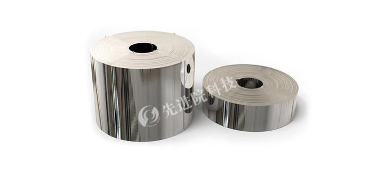
However, the inherent insulation and surface inertness of PEEK film pose technical bottlenecks in applications that require conductivity, electromagnetic shielding, or signal transmission functions. Among them, the poor adhesion of titanium plating on the surface of PEEK film, its inability to withstand bending, and its difficulty in continuous production have been pain points that have plagued the industry for many years. Advanced Institute (Shenzhen) Technology Co., Ltd. (hereinafter referred to as "Advanced Institute Technology") focuses on the research and industrialization of surface metallization technology for polymer materials, and has mastered multiple independent core processes in the fields of special thin film titanium plating, copper plating, and alloying functional layers. The company is based on self-developed“Low temperature gradient interface locking”The technology has successfully achieved mass production of titanium coated PEEK film rolls with a width of 600mm and a film thickness as low as 6 μ m. It can provide stable and customizable conductive functional film solutions for medical, 5G communication, aerospace, and high-end electroacoustic fields.
1、 Process Challenge: Non stick Characteristics of PEEK Film and Low Temperature Requirements
PEEK film has excellent high-temperature resistance (continuous use temperature can reach 250 ° C, short-term heat resistance can exceed 300 ° C), chemical corrosion resistance, high mechanical strength, and low dielectric loss, making it an ideal substrate for applications such as implantable sensors, flexible circuit boards, and satellite thermal control components.
However, PEEK film has extremely low surface energy, high crystallinity, and strong chemical inertness, making it difficult for metal coatings to directly adhere. The biological inertness of PEEK is one of its main weaknesses as an implant material - it cannot directly bond with bones and lacks bone integration ability. Therefore, PEEK film must undergo surface activation treatment before undergoing metalization processes such as chemical plating or physical vapor deposition.
Traditional plastic metallization processes often use high-temperature fusion or strong acid roughening treatment. Chemical roughening usually uses chromic acid sulfuric acid system or potassium permanganate system to etch micro pits on the surface of PEEK, while introducing polar groups to enhance surface energy. However, the glass transition temperature of PEEK is only around 143 ℃. Excessive temperature or intense chemical reactions can easily cause film deformation, brittleness, loss of flexibility and dimensional accuracy. If titanium is directly sputtered at low temperatures to avoid thermal damage, it is difficult for titanium atoms to form chemical bonds with the surface of PEEK, resulting in a loose film layer that peels off with slight external force and cannot pass repeated bending or long-term implantation testing.
Key bottleneck:The surface metallization of PEEK film usually involves three key steps: surface activation pretreatment, establishment of conductive layer, and deposition of functional layer. Any problem at any stage can lead to coating peeling or substandard performance.
2、 Core technology: Low temperature gradient interface locking process
The "Low Temperature Gradient Interface Locking" technology independently developed by Advanced Institute Technology has achieved high-strength bonding between titanium coating and PEEK substrate at process temperatures below 120 ℃ through three key steps:
1.Online plasma surface activation
Pre treatment of PEEK film surface using plasma in a vacuum environment. Advanced Institute Technology has found in process practice that plasma activation combined with low-energy ion beam pretreatment can effectively shorten the induction time of subsequent chemical plating, and has a smaller impact on the mechanical properties of the film itself. This process constructs a nanoscale micro rough morphology on the surface of the film, while introducing a large number of oxygen-containing and nitrogen-containing active functional groups to provide sites for subsequent chemical bonding.
2.Low temperature and high ionization gradient transition layer deposition
At process temperatures below 120 ℃, a thickness controllable titanium/titanium carbide (Ti/TiC) gradient transition layer is deposited using high ionization pulse magnetron sputtering technology. Compared with traditional chemical plating methods, PVD technology has advantages such as environmental protection, good coating uniformity, and strong adhesion. It can achieve uniform deposition of metal atoms on the substrate surface under low temperature conditions. The transition layer forms a dense chemical bond and mechanical interlocking structure at the interface, like a "nano anchor" firmly anchoring the PEEK substrate, while the other side provides a dense metal substrate for the continuous growth of pure titanium functional layers. Magnetron sputtering technology can deposit titanium thin films at low temperatures, making them suitable for coatings that require high hardness and chemical inertness.
3.Growth of pure titanium functional layer
Continue to deposit a pure titanium layer on top of the transition layer, with a thickness that can be precisely controlled between 50 nanometers and 3 micrometers according to application requirements. The titanium layer is dense and uniform, and the surface can be further anodized or functionalized. Relying on advanced physical vapor deposition (PVD) technology, the company has achieved nanometer level accurate control of metal thin films on substrate surfaces, ensuring extremely high uniformity and density.
Key performance indicators
adhesionISO 2409 grid division method level 0 (grid 5B)|
peel strength≥ 0.8 N/mm (ASTM D3359) |
Flexible resistance>1 million times (R<1mm) resistance change<5%
The titanium coated PEEK film produced by this process has achieved the highest adhesion level of 0 (5B per hundred grids) according to the ISO 2409 grid method test, and the peel strength exceeds 0.8 N/mm according to relevant standards such as ASTM D3359. After millions of flexural tests (bending radius<1mm), the resistance change rate of the conductive path is less than 5%, fully meeting the reliability requirements in dynamic bending scenarios.
3、 Roll to roll continuous titanium plating production line and quality control
Established in 2016, Advanced Institute Technology is headquartered in Bao'an District, Shenzhen, Guangdong Province. It is a national high-tech enterprise focusing on shielding materials, insulation materials, thermal conductivity materials, and precious metal coatings. The company has its own registered trademark "Research Platinum" and has dual production bases in Shenzhen and Dongguan. The company's R&D team has independent research and development capabilities in the fields of flexible substrate coating, electronic paste, electromagnetic shielding materials, etc.
The company has independently built a magnetron sputtering and vacuum evaporation production line, using roll to roll continuous production technology, which can continuously and uniformly deposit metal layers on the surface of flexible polymer films. Suitable substrates include various flexible materials such as FEP, PI, PET, LCP, PPS, PEN, PP, etc., and can be plated with metals including gold, silver, copper, aluminum, tin, nickel, titanium, platinum, etc.
| project |
parameter |
| Applicable substrates |
Special polymer films such as PEEK and PI |
| Maximum width |
600mm |
| Thickness of basement membrane |
Minimum processing capacity of 6 μ m |
| process temperature |
Full process closed-loop temperature control within 130 ℃ |
| Whole roll performance fluctuation |
Control within ± 5% |
The closed-loop temperature control throughout the entire process ensures that the film surface is free from thermal wrinkles and shrinks, and is smoothly rolled up. Integrated spectral reflectance film thickness monitoring system on the production line, real-time tracking of the square resistance and optical characteristics of each meter of thin film. The full vacuum dry process has no discharge of wastewater, waste acid, or organic solvents, complies with the RoHS directive, and can meet the requirements of ISO 10993 for biological evaluation of medical devices.
Qualification Certification
The company has passed ISO9001 quality management system certification, and its products comply with GJB 773A aerospace related standards and RoHS environmental requirements. It has the ability to support high-end fields such as aerospace, military, and 5G communication. The national standard GB/T 43763-2024 "Aerospace Functional Coatings - Special Non Metallic Materials - Metal Coatings" has clearly stipulated that various metal coatings can be prepared on the surface of special non-metallic materials such as PEEK using electroplating or chemical plating methods.
Customization capability
The thickness of the titanium layer can be customized to any specification from 50nm to 3 μ m, and supports co deposition of functional elements such as silver and copper in the titanium layer, endowing the film with composite properties such as antibacterial, high conductivity, and thermal conductivity. At the same time, we can provide customers with secondary processing services such as photolithography patterned titanium plating, gradient photoresist, etc., to achieve material integration with terminal processes from the factory.
4、 Typical application areas
�� Medical devices and brain computer interfaces
Titanium coated PEEK film is processed by laser microfabrication to produce flexible neural electrodes, electrocorticography arrays, or implantable sensor substrates. The low impedance interface of the titanium layer ensures high fidelity signal transmission, and the surface titanium oxide layer provides a biologically inert barrier to reduce rejection reactions.
�� 5G and Flexible Electronics
As a transitional bonding layer for flexible copper-clad laminates (FCCL), the titanium layer significantly enhances the peel strength between the copper foil and PEEK substrate, meeting the high-frequency, low loss, and high flexural resistance requirements for foldable screen phones, VR/AR antennas, and other applications. The dielectric loss of PEEK film can be as low as around 0.0035 in the 20 GHz frequency band.
��️ Aerospace lightweighting
Titanium coated PEEK film is used as the outer layer of multi-layer insulation components and lightweight electromagnetic shielding film for satellites. The titanium layer endows high solar reflectivity and excellent resistance to atomic oxygen erosion, significantly reducing the structural weight.
�� High end electroacoustic devices
The titanium/PEEK composite diaphragm combines the high stiffness of titanium metal with the high internal friction characteristics of PEEK, which can improve the frequency response flatness of headphones and micro speakers and reduce harmonic distortion.
About Advanced Institute (Shenzhen) Technology Co., Ltd
Advanced Institute Technology is a high-tech enterprise dedicated to surface functionalization and metallization technology of polymer materials. The core team has many years of engineering experience in vacuum plasma surface modification, magnetron sputtering film preparation, and other fields. The company has integrated the entire chain from film material evaluation, interface process development, small-scale trial production to roll to roll mass production, and can provide high-performance coating products and joint research and development services for customers in industries such as medical equipment, communication equipment, aerospace, and consumer electronics.
Obtain technical information, conduct sample testing, and negotiate cooperation
Inquiry hotline:0755-22277778
mobile phone13826586185 (Mr. Duan)
Address:8th Floor, Zhongxing Building, Xinsha Road, Xinqiao Street, Bao'an District, Shenzhen
Advanced Institute Technology is committed to becoming a reliable partner in the field of special functional thin film metallization, helping customers achieve material innovation and cost optimization in the new generation of high-end manufacturing.
2026 Advanced Institute (Shenzhen) Technology Co., Ltd. All rights reserved
 en
en  Español
 Français
 Português



