1、 What is an "electromagnetic wave suppression absorbing plate" - understanding the technical logic from its functional positioning
Electromagnetic wave suppression absorbing plate is essentially a functional sheet that absorbs electromagnetic interference rather than reflecting it. The core difference between it and traditional electromagnetic shielding materials lies in its working mechanism: shielding materials reflect electromagnetic waves back through conductive layers, while absorbing wave plates convert electromagnetic wave energy into thermal energy and dissipate it through magnetic and dielectric loss mechanisms. This difference determines that absorption plates have irreplaceable advantages in suppressing near-field noise, eliminating cavity resonance, and improving signal integrity.
Electromagnetic wave suppression absorbing plates are usually composed of magnetic fillers (such as sheet-like soft magnetic alloy powder, carbonyl iron powder, etc.), polymer substrates (such as silicone rubber, acrylic resin, etc.), and composite absorbing layers. The core of its technology lies in uniformly dispersing micrometer sized sheet-like magnetic particles in a polymer matrix to form a three-dimensional magnetic loss network. When electromagnetic waves are incident on the surface of a material, magnetic particles undergo magnetization response in an alternating electromagnetic field, converting electromagnetic energy into thermal energy through mechanisms such as hysteresis loss, eddy current loss, and natural resonance. Research has shown that sheet-like magnetic absorbers can break through the Snoek limit due to their shape anisotropy, achieving higher magnetic permeability and better absorption performance in the GHz frequency band.
2、 Performance leap: technological breakthrough from ultra-thin to broadband absorption
In 2026, the technological evolution of electromagnetic wave suppression absorbing plates will show several clear directions.
Ultra thin and flexible are the most significant trends. As the internal space of electronic devices continues to compress, the thickness of absorbing wave plates is crossing from the millimeter level to the micrometer level. The thickness of the flexible radio wave absorber developed by MEKTEC company has exceeded 0.1mm, and the FPC manufacturing process has been used to achieve ultra-thin, lightweight, and high flexibility design, which can be installed in narrow spaces and complex curved surfaces. The thickness of the nano carbon electromagnetic wave suppression sheet developed by Hokuetsu Corporation in Japan is only 40 μ m. The ultra-thin design enables the absorption plate to be easily attached to the surface of chips, flexible circuit boards, and even inside wearable devices, achieving noise suppression with almost no increase in thickness.
Broadband absorption capability is shifting from a "bonus point" to a "standard feature". The interference spectrum of modern electronic devices has extended from 100MHz to millimeter wave frequency band. Hokuetsu's nanocarbon suppression sheet can absorb conductive noise in the 1GHz-30GHz frequency range and suppress radioactive noise in the 100MHz-3000GHz range. MEKTEC's products use metamaterial technology to achieve a noise absorption rate of over 99% in the 28GHz frequency band. PPG's C-RAM FLX flexible microwave absorbing sheet can absorb up to 99% of incident RF energy within the specified frequency range of 1-35GHz. The continuous expansion of broadband absorption capability enables electromagnetic wave suppression absorbing plates to simultaneously respond to composite electromagnetic interference from different frequency bands and sources.
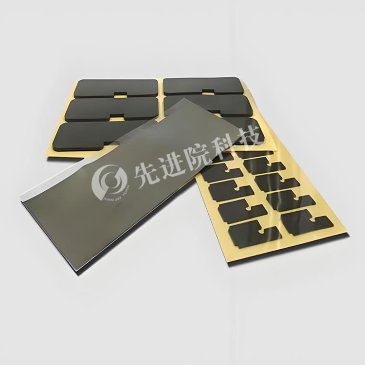
Convenience and integrability are equally key considerations. Modern electromagnetic wave suppression absorbing plates are usually supplied in the form of tape or strip, with an acrylic pressure-sensitive adhesive layer at the bottom, which can be directly attached to the surface of noise sources or sensitive devices. This "plug and play" feature significantly reduces the threshold for electromagnetic compatibility design - engineers do not need to redesign shielding covers or metal cavities, only need to attach absorbing wave plates at critical locations to achieve significant noise suppression effects.
3、 Three core application scenarios: from smartphones to humanoid robots
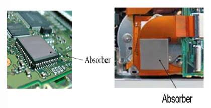
Smartphones and consumer electronics are the fields with the highest usage of electromagnetic wave suppression absorbing plates. In devices such as smartphones, tablets, and digital cameras, RF modules, antennas, camera modules, and display driver chips are densely arranged in small spaces, and electromagnetic coupling and near-field noise interference between them have become key bottlenecks affecting signal integrity and user experience. Electromagnetic wave suppression absorbing plates can be directly attached to noise sources (such as DC/DC converters, RF power amplifiers) or sensitive circuits (such as antenna feed points, sensor interfaces), effectively absorbing near-field noise, suppressing resonance, and reducing crosstalk. In wireless charging scenarios, absorbing plates can also improve charging efficiency by guiding magnetic flux and reducing leakage magnetic fields. With the emergence of new forms of consumer electronics such as foldable screen smartphones and AR/VR devices, the demand for ultra-thin and flexible wave absorbing plates is accelerating.
5G/6G communication and network devices represent the most technically demanding application direction. The operating frequency of 5G millimeter wave and future 6G communication systems has climbed to 28GHz or even higher, and electromagnetic radiation interference between internal modules of devices has become a core challenge affecting system stability. Electromagnetic wave suppression absorbing plates are widely used in 5G base stations, RF front-end modules, filters, high-speed communication equipment, and other scenarios to absorb stray electromagnetic waves inside cavities, suppress resonance, and reduce noise. In the millimeter wave frequency band, the introduction of metamaterial structures enables the absorption plate to achieve "selective tuning" for specific frequency bands - through fine circuit design, the absorption plate can achieve an absorption rate of over 99% in the target frequency band. This has significant engineering value for high-frequency communication equipment that needs to meet strict EMC standards.
Automotive electronics and intelligent driving are the fastest-growing application directions. Car infotainment systems, wireless communication modules, control units, etc. have strict requirements for electromagnetic compatibility. The noise suppression film certified by AEC-Q200 automotive standards has been widely used in automotive scenarios. In millimeter wave radar modules (24GHz, 77GHz, and other frequency bands), electromagnetic wave suppression absorbing plates can be used to suppress cavity resonance, reduce sidelobe interference, and prevent ghosting phenomena (the radar misjudges multipath interference as false targets). With the intensive integration of servo motors, sensors, and communication modules in humanoid robots and next-generation high-speed communication devices, the demand for flexible and ultra-thin wave absorbing plates is also rapidly increasing.
4、 Selection points and design suggestions
When selecting electromagnetic wave suppression absorbers, engineers need to focus on the following dimensions: matching the operating frequency band - the optimal absorption frequency band for different material systems and structural designs is different, and it needs to be matched according to the main interference frequency of the equipment (from MHz to millimeter waves); Thickness and installation space - ultra-thin (<0.1mm) is suitable for extremely limited space scenarios such as mobile phones and wearable devices, while thicker (0.1-0.5mm) is suitable for communication and automotive electronics scenarios that require higher absorption efficiency; Environmental tolerance - requires evaluation of working temperature range, flame retardant rating (such as UL94 V-0), and weather resistance requirements; Installation method - whether adhesive backing is required, whether customized size and shape are needed; Balance between shielding and absorption - Some products have a certain degree of reflection (shielding) performance while absorbing, which needs to be comprehensively evaluated based on specific EMC requirements.
Advanced Institute Technology provides full process technical support from material selection, performance testing to sample trial production and batch delivery, helping customers incorporate electromagnetic wave suppression absorption plate solutions into overall electromagnetic compatibility considerations in the early stages of product design.
5、 Outlook
The global RF absorbing plate market is expected to continue expanding at a compound annual growth rate of 7.8%, from $386 million in 2025 to $656 million in 2032. The global market for electromagnetic wave absorbing materials has reached 5.06 billion US dollars by 2025 and is expected to exceed 7.58 billion US dollars by 2030. Driven by the continuous deployment of 5G/6G communication infrastructure, the lightweight and high-frequency development of consumer electronics, the deep evolution of automotive intelligence and electrification, and the accelerated emergence of emerging applications such as humanoid robots, electromagnetic wave suppression absorbing plates are moving from "professional material selection" to standard configuration for electromagnetic compatibility design of electronic devices.
At the same time, the industry is continuously evolving towards thinner, softer, wider, and smarter directions. Cutting edge technologies such as metamaterial absorbing structures, nanocrystalline magnetic materials, and multifunctional integrated absorbing plates (combining thermal conductivity, insulation, and absorption) are constantly expanding the performance boundaries of electromagnetic wave suppression absorbing plates. Advanced Institute (Shenzhen) Technology Co., Ltd. will continue to deepen its expertise in the field of electromagnetic wave suppression and absorption materials, providing customers with higher performance and more reliable electromagnetic compatibility solutions through material innovation and process optimization.
 en
en  Español
 Français
 Português



