In the field of electronic materials, the demand for high-performance thin film materials is growing exponentially with the development of technology. among which,PI copper plated filmWith its unique performance advantages, it has become a key material in cutting-edge fields such as flexible circuits and high-frequency communication. The PI copper plated film produced by Advanced Institute Technology achieves a perfect combination of copper layer and PI substrate through vacuum sputtering technology, setting a new performance benchmark for the industry.
Vacuum Sputtering: The Technological Password for Precision Manufacturing
The core process of PI copper plating film lies in vacuum sputtering technology. This process is completed in a highly clean vacuum environment, accelerating inert gas ions through a high-voltage electric field to bombard the surface of the copper target at extremely high speeds. Copper atoms or molecules on the surface of the target material gain escape kinetic energy through energy transfer, forming a directed flow of copper particles. After passing through the vacuum chamber, these particles uniformly deposit on the surface of the PI film, forming a controllable thickness copper layer.
The breakthrough of this technology lies in achieving nanoscale precision in coating control. Advanced Institute Technology adopts a multi-target co sputtering system, which can accurately control the deposition rate and crystal structure of copper layers by adjusting parameters such as electric field strength and gas pressure. Experimental data shows that the thickness deviation of the copper plated film produced by it is controlled within ± 0.5 μ m, and the surface roughness Ra value is less than 30nm, fully meeting the strict requirements of 5G communication equipment for signal integrity.
Performance Fusion: A Material Revolution of 1 1>2
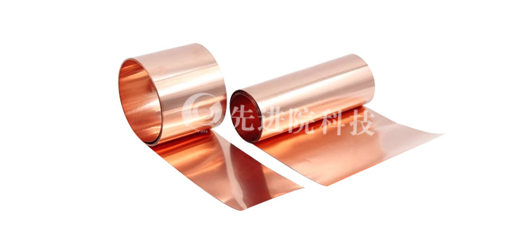
PI film itself has excellent high temperature resistance (long-term use temperature up to 260 ℃), mechanical strength (tensile strength>200MPa), and electrical insulation (volume resistivity>10 ¹⁶Ω· cm). The copper layer deposited by vacuum sputtering technology endows it with excellent conductivity (conductivity>98% IACS) and electromagnetic shielding effectiveness (> 80dB@1GHz ). The organic fusion of this performance makesPI copper plated filmBecoming an ideal choice for fields such as flexible printed circuit boards (FPC) and lithium-ion battery current collectors.
The innovation of Advanced Institute Technology lies in solving the inherent defects of traditional electroplating processes. The vacuum sputtering process does not require the use of chemical plating solution, completely avoiding interface contamination between the copper layer and the PI substrate. X-ray diffraction analysis shows that the copper layer exhibits a preferred orientation of (111) crystal planes, which significantly improves the fatigue resistance of the copper layer. After 100000 bending tests, it still maintains a complete conductive path.
Customized service: Accurately matching customer needs
For different application scenarios, Advanced Institute Technology provides customized services with a full thickness range of 5 μ m to 125 μ m. In the case of a research institute in Lanzhou, the client needs to develop an extremely thin copper plating film (thickness 8 μ m) for high-energy physics detectors. By optimizing the sputtering power and substrate temperature parameters, the R&D team successfully achieved gradient bonding between the copper layer and the PI substrate, ensuring both the signal transmission efficiency of the detector and the flexibility of the substrate.
This customization capability comes from advanced production equipment and process databases. The roll to roll vacuum sputtering production line equipped by the enterprise can achieve continuous production, with an annual production capacity of 500000 square meters per line. At the same time, the established process parameter model covers more than 200 material combination schemes, which can quickly respond to special needs in fields such as aerospace and new energy vehicles.
From laboratory research to large-scale production,Advanced Institute of TechnologyThe PI copper plated film is reshaping the electronic materials industry landscape. Its vacuum sputtering technology not only breaks through the performance bottleneck of traditional processes, but also provides key material support for high-end equipment manufacturing through precise customized services. With the popularization of emerging technologies such as 5G and the Internet of Things, this composite material that combines high performance and flexibility is bound to have broader application prospects.

 en
en  Español
 Français
 Português



