1、 What does 2.3 μ m mean? ——What challenges does the coating process face when the substrate approaches its physical limit
The thickness of PET film is continuously evolving from 4.5 μ m to 3 μ m. 2.3μm, It means being one size thinner than the industry mainstream.
On the roll to roll continuous coating production line, the 2.3 μ m PET substrate is a "dangerous" presence - it can break under slightly high tension, shrink at slightly high temperatures, and wrinkle at slightly faster speeds. The PET copper plated film with conventional thicknesses (such as 25 μ m and 50 μ m) is quite mature, but compressing the substrate thickness to 2.3 μ m no longer poses a challenge of "whether it can be plated", but "whether it can still be used after plating".
Advanced technology has solved this problem. The company uses vacuum magnetron sputtering technology in physical vapor deposition (PVD) to sputter high-purity oxygen free copper atoms onto the surface of PET film in a highly vacuum environment, forming a uniform and dense copper layer. The thickness of the copper layer can be accurately controlled, and the resistance can be flexibly adjusted within the range of 0.01-1 Ω/□ according to demand. In response to the special challenges of the 2.3 μ m ultra-thin substrate, the company has achieved precise control in tension control, temperature control accuracy, and coating uniformity, ensuring that every meter of product can withstand inspection.
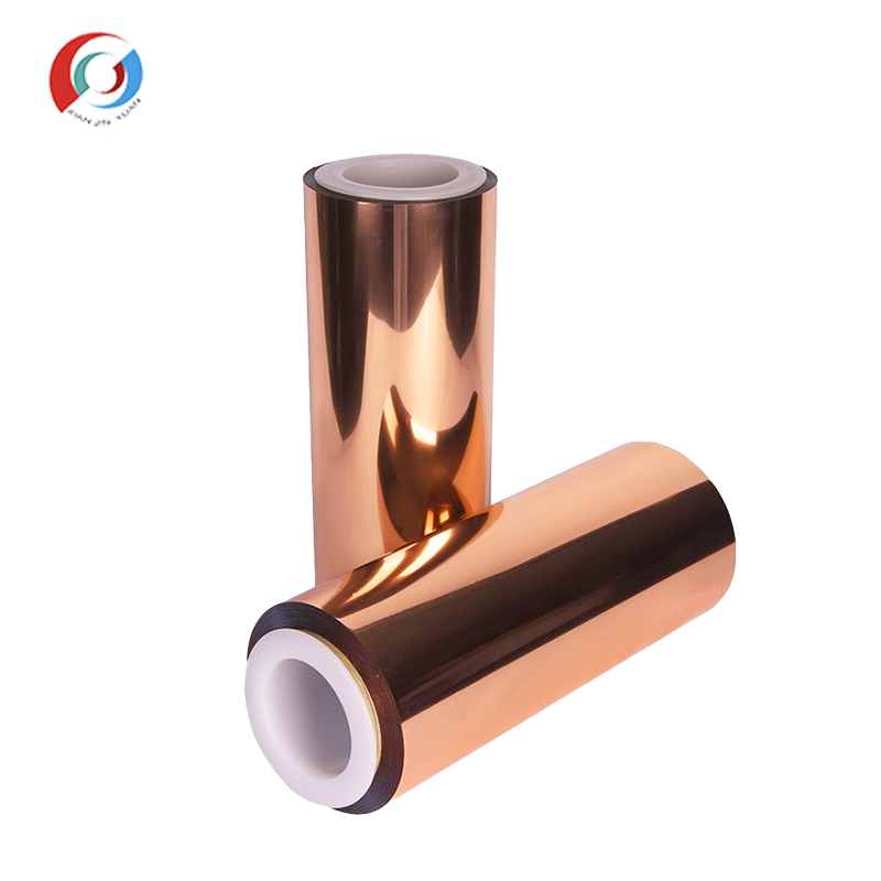
2、 Data Speaking: 0.3 μ m Copper Layer, 225m Ω Square Resistance - The "Optimal Solution" for Conductivity Performance
In the advanced technology 2.3 μ m PET copper plated film product series, the 2.3 0.3PET copper plated film is undoubtedly the main promoted model - with a copper layer thickness of 0.3 μ m and a measured square resistance as low as 225m Ω, it is the most conductive among the four models.
There is a subtle balance between the thickness of the copper layer and the square resistance. The thicker the copper layer, the denser the conductive channels, and the lower the square resistance should be - but the measured square resistance of 2.3 0.7PET copper plated film (copper layer 0.7 μ m) is 380m Ω, which is higher than the 225m Ω of the 0.3 μ m model. This is not abnormal, but the result of the combined effect of copper layer grain structure and deposition process - an excessively thick copper layer may cause grain coarsening on ultra-thin substrates due to stress accumulation, which in turn affects the efficiency of conductive pathways. 0.3 μ m precisely finds the "sweet spot" of performance: it ensures the continuity and density of the copper layer, while avoiding stress problems caused by excessive thickness.
The value of a 0.3 μ m copper layer goes beyond conductivity. On a 2.3 μ m ultra-thin substrate, every 0.1 μ m increase in copper layer thickness will affect the flexibility and bending life of the material. 0.3 μ m achieves the optimal balance between conductivity and flexibility - providing sufficiently low resistance to meet circuit transmission requirements while maintaining the ultimate bending ability of ultra-thin substrates.
3、 Application boundary of 0.3 μ m copper layer: when both "thin" and "conductive" become essential
Flexible circuits and foldable screen devices are the most representative application scenarios for 2.3 0.3 PET copper plated film. The internal wiring of foldable screen phones needs to transmit signals in extremely thin spaces and withstand hundreds of thousands of bends. The combination of a 2.3 μ m ultra-thin substrate and a 0.3 μ m copper layer significantly reduces the thickness of the wiring, freeing up critical space for the design of hinge mechanisms. The global flexible electronic product market is expected to exceed 87 billion US dollars by 2030, and the demand for PET composite copper plated materials continues to rise.
Wearable devices and microsensors are the most prominent areas of "invisible value" for 0.3 μ m copper layers. The internal space of smartwatches, TWS earphones, and medical sensors is more cramped than that of mobile phones, and every 0.1mm increase in thickness may affect wearing comfort or battery capacity. The ultra-thin characteristics of 0.3 PET copper plated film make it an ideal conductive substrate for these scenarios - with no compromise in conductivity and almost no increase in thickness.
Electromagnetic shielding and lightweight design also benefit from the precise thickness of the 0.3 μ m copper layer. In situations that require electromagnetic shielding but are sensitive to weight, such as cable shielding layers inside drones and EMI protection for portable electronic devices, a 0.3 μ m copper layer ensures shielding effectiveness while minimizing weight gain. The surface density of PET/Cu composite foil can be reduced by 44.89% compared to pure copper foil. In the field of power battery current collectors, the quality of PET composite current collectors is only 30% of that of commercial copper foils.
4、 Product matrix: 0.3 μ m is the main promotion, with more options available
0.3 μ m is the main recommended model in the Advanced Institute Technology 2.3 μ m PET copper plated film series, but it is not the only choice. The company also offers the following customization options:
2.3 0.1PET copper plated film (copper layer 0.1 μ m, measured square resistance 520m Ω): extremely lightweight and suitable for scenarios with extremely high bending life requirements
2.3 0.07PET copper plated film (copper layer 0.07 μ m, measured square resistance 500-700m Ω): ultra-thin conductive layer with minimal impact on substrate flexibility
2.3 0.7PET copper plated film (copper layer 0.7 μ m, measured square resistance 380m Ω): highly reliable and durable, suitable for scenarios requiring certain structural strength
Different copper layer thicknesses correspond to different square resistance properties and application scenarios. Advanced Institute Technology supports on-demand customization, accurately matching customers' differentiated needs. The company has passed ISO9001 certification and its products comply with RoHS environmental requirements.
The global PET composite copper foil industry will enter a stage of large-scale production in 2025, with annual shipments exceeding 1.2 billion square meters. The global PET composite copper plating market has reached 1.12 billion US dollars by 2025 and is expected to grow to 1.8 billion US dollars by 2033. Driven by the popularization of foldable screens, the explosion of wearable devices, the lightweighting of power batteries, and the high frequency of consumer electronics, the 2.3 μ m ultra-thin PET copper plated film is moving from "extreme manufacturing" to a standard option for multifunctional substrates in multiple fields.
Advanced Institute (Shenzhen) Technology Co., Ltd. will continue to deepen its cultivation in the field of ultra-thin PET copper plated film, providing customers with higher performance and more reliable flexible substrate conductive solutions through precision coating technology and continuous technological innovation.

 en
en  Español
 Français
 Português



