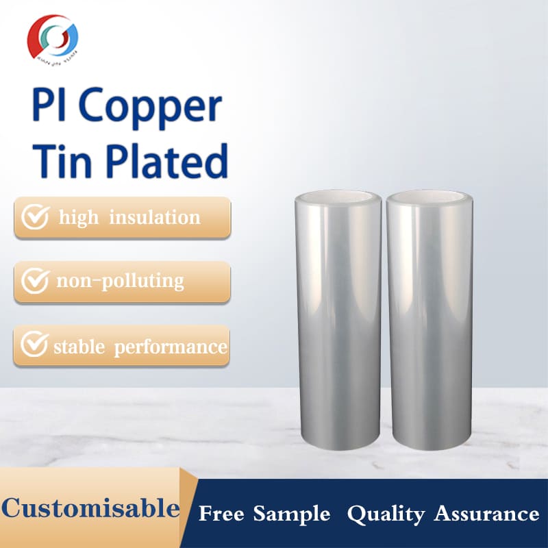
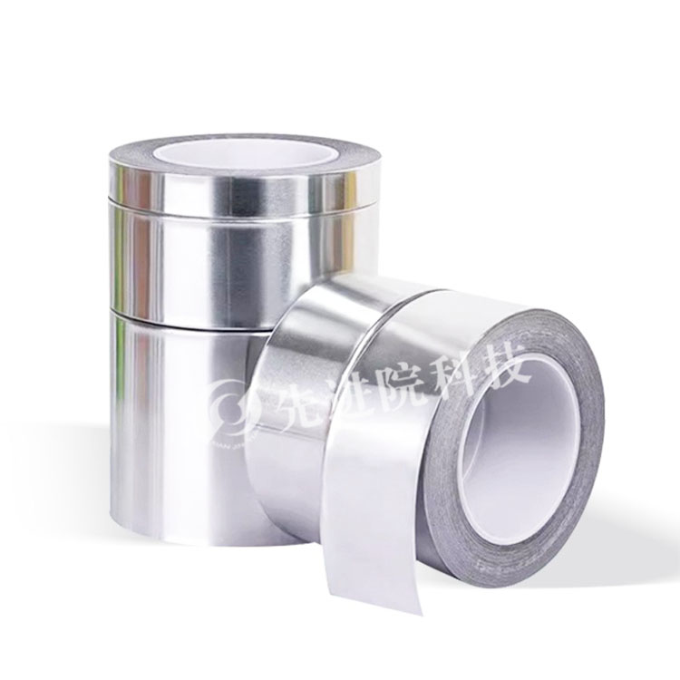
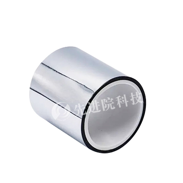
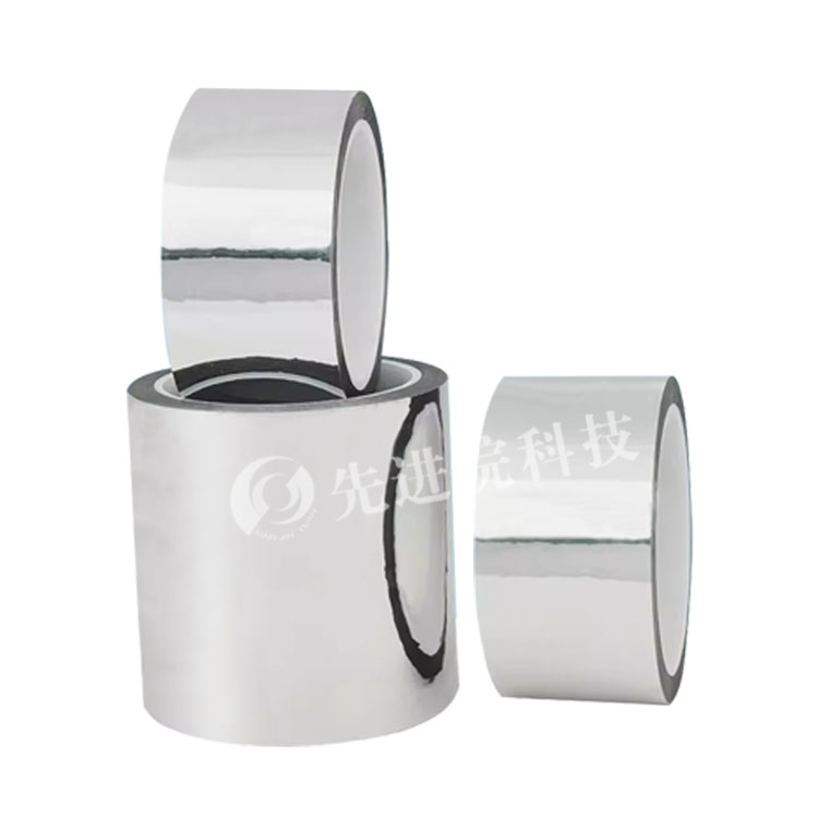
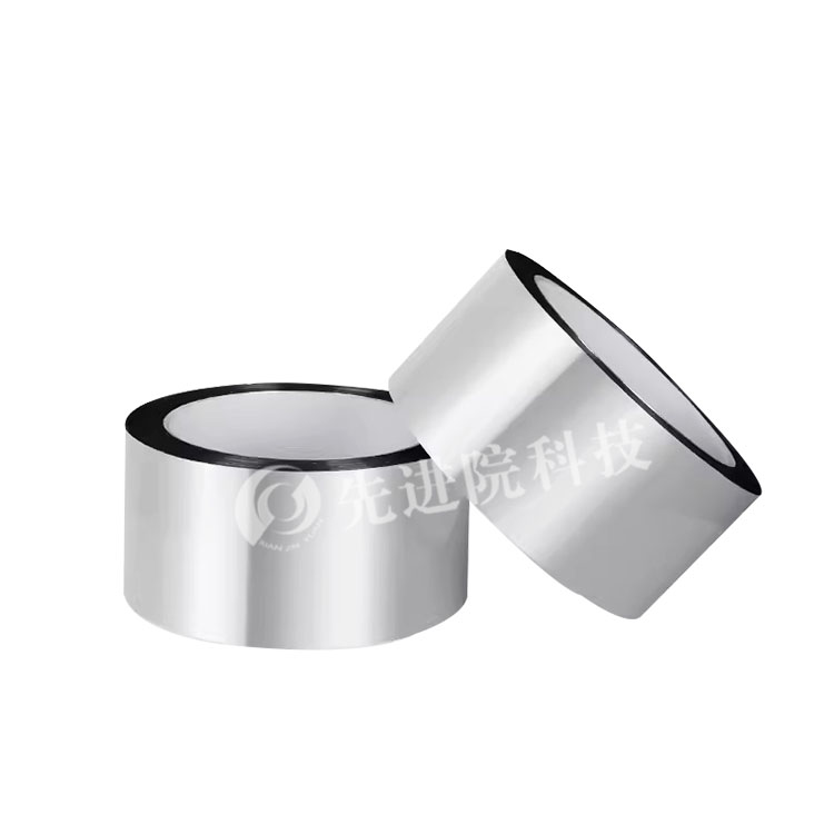
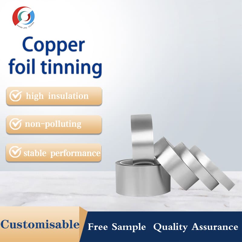
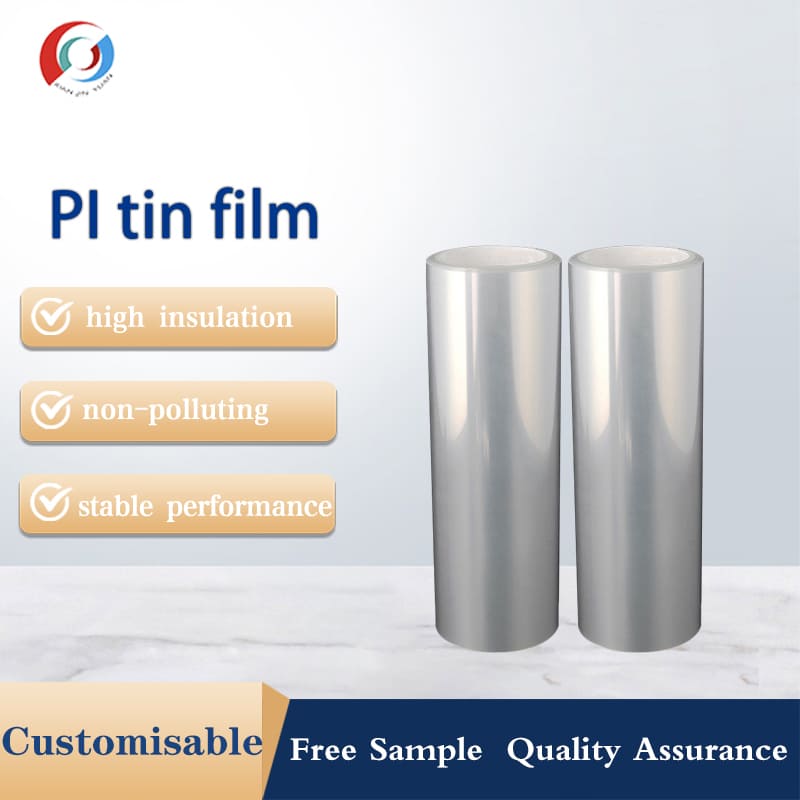
PI copper plated tin plated film is a high-performance composite material that combines the excellent properties of polyimide (PI) film with the conductivity and corrosion resistance of metal copper and tin, forming a material with broad application prospects in multiple fields such as electronics, aerospace, medical equipment, etc.
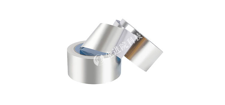
Characteristics of flexible copper plated tin plated sheet products
Excellent conductivity: The copper coating endows the PI copper plated tin plated film with excellent conductivity, enabling smooth current conduction in the material, reducing energy loss, and improving the response speed and operating efficiency of electronic products.
High temperature stability: The excellent high temperature stability of PI substrate enables PI copper plated tin plated film to maintain stable performance in high temperature environments, without deformation or damage, making it suitable for applications that require high temperature resistance.
Good corrosion resistance: Tin plating has good corrosion resistance to various chemicals, which can effectively prevent the corrosion and damage of copper layers and PI substrates in harsh environments, and extend the service life of products.
Easy to solder: The tin coating improves the welding performance of the material, making it easy to solder PI copper plated tin plated film in the manufacturing and maintenance process of electronic products, improving production efficiency and product quality.
Excellent bending resistance: The excellent mechanical properties of PI substrate make PI copper plated tin plated film have good bending resistance, which can adapt to various complex bending and twisting environments, ensuring the stability and reliability of the product.
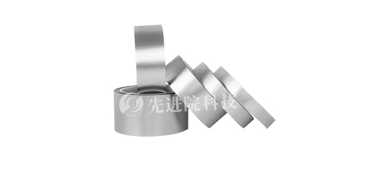
Production process of solderable flexible circuit substrate
PI film preparation: High quality PI films are prepared as substrates through specific processes.
Copper plating treatment: A uniform and dense copper layer is deposited on the surface of PI film by electroplating or chemical plating methods.
Tin plating treatment: Continuing to deposit a uniform and dense layer of tin on the surface of the copper layer through electroplating or chemical plating methods.
Post treatment: Clean, dry, and cure the PI film after copper plating and tin plating to ensure the stability and consistency of product quality.
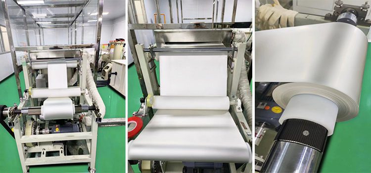
Workshop Display
Overview of the application fields of PI copper plated tin plated composite film
1、 Advanced semiconductor packaging and hybrid bonding
This field is the most advanced application of this material, mainly used to achieve ultra-high density and high-performance three-dimensional interconnection between chips.
Wafer level/chip level hybrid bonding: This material is the key to achieving "copper/polymer hybrid bonding" or "polymer/metal hybrid bonding". PI serves as an insulating medium, and the copper tin layer on the surface can form copper tin eutectic bonding (Cu/Sn eutectic bonding) under hot pressing, thereby achieving electrical and mechanical connections simultaneously in a single process. This technology is the core of implementing advanced packaging such as 2.5D/3D IC and high bandwidth memory (HBM).
Ultra high density interconnect and rewiring layer: This material can be used to create rewiring layers (RDL) with extremely small line width/spacing, providing high-density interconnects for chips. The combination of photosensitive polyimide and copper tin metallization can support high-resolution structures with line widths ≤ 5 μ m.
2、 High reliability flexible circuits and electronics
This field mainly utilizes its composite functions to achieve high reliability soldering, shielding, or special interconnection on flexible circuits.
High temperature resistant soldering type flexible printed circuit board: used for making flexible circuit boards (FPCs) that require high-temperature soldering processes such as reflow soldering. The tin layer provides long-term oxidation protection and excellent solderability for the solder pad, while the underlying copper ensures high conductivity of the circuit, and the PI substrate ensures overall dimensional stability during the soldering process.
Flexible electromagnetic shielding and grounding: It can be made into flexible electromagnetic shielding film or grounding sheet with high shielding efficiency. The copper layer provides the main conductive shielding function, while the tin layer enhances the resistance to environmental corrosion.
High reliability sensors and interconnect components: used in harsh environments such as automotive electronics and aerospace to manufacture high-speed interconnect jumpers or electrical contacts between flexible sensor circuits and modules, ensuring long-term stable electrical performance.
3、 High temperature, high reliability special applications
Combined with the overall environmental resistance characteristics of the material, it is suitable for extreme working conditions.
Electrical connection and thermal management in high temperature environments: used in aerospace and high-end industrial equipment as interface materials or connection components that require conductivity, thermal conductivity, and weldability simultaneously.
Special packaging and sealing components: Utilizing the characteristics of copper tin eutectic bonding, they can be used for airtight packaging of microdevices or high-strength sealing connections between metals and polymers.
Core advantages and selection considerations
Functional integration: A single material simultaneously solves the three major requirements of conductivity (copper), solderability/bonding (tin), and insulation/support (PI), simplifying design and assembly processes.
High reliability: The system formed by PI and copper tin metal layer can pass strict thermal cycling and high humidity reliability testing, suitable for long-life and high demand products.
Process compatibility and progressiveness: highly compatible with semiconductor and precision electronic manufacturing processes, it is one of the leading materials to realize the next generation of advanced packaging technology (such as hybrid bonding).

 en
en  Español
 Français
 Português