Polyether ether ketone (PEEK)Known as the "pyramid tip" of the special engineering plastics family. As a semi crystalline thermoplastic special engineering plastic, PEEK has been widely used in aerospace, electronic and electrical, medical equipment, and new energy fields due to its excellent high temperature resistance, mechanical strength, chemical stability, and electrical insulation properties. PEEK film can operate stably in environments above 250 ° C for a long time, with a stable dielectric constant of around 3.2 and a dielectric loss tangent value as low as 0.0015 in the 1-10 GHz frequency band, making it an ideal dielectric material for high-frequency signal transmission scenarios. However, the inherent insulation and surface inertness of PEEK film pose technical bottlenecks in applications that require conductivity, electromagnetic shielding, or signal transmission functions. Advanced Institute (Shenzhen) Technology Co., Ltd. is deeply engaged in the field of PEEK film metallization, with independent research and developmentPlasma activated magnetron sputteringCraftsmanship is the core, providing a one-stop PEEK film metallization solution for high-end manufacturing.
1、 Company Overview and Technical Positioning
Advanced Institute (Shenzhen) Technology Co., LtdEstablished in 2016, headquartered in Bao'an District, Shenzhen, Guangdong Province, we are a national high-tech enterprise focusing on shielding materials, insulation materials, thermal conductive materials, and precious metal coatings. The company has its own registered trademark "Research Platinum" and has dual production bases in Shenzhen and Dongguan. It has passedISO9001Quality management system certification, products comply withGJB 773AAerospace related standards andRoHSEnvironmental protection requirements, with the ability to support high-end fields such as aerospace, military, and 5G communication.
In the field of coating technology, the company has independently built magnetron sputtering and vacuum evaporation production lines, usingContinuous production process of roll to rollIt can continuously and uniformly deposit metal layers on the surface of flexible polymer films. Suitable substrates include various flexible materials such as FEP, PI, PET, LCP, PPS, PEN, PP, etc., and can be plated with metals including gold, silver, copper, aluminum, tin, nickel, titanium, platinum, etc. Relying on advanced physical vapor deposition (PVD) technology, the company has achieved nanometer level precise control of metal thin films on the substrate surface, with thickness ranging from a few nanometers to several hundred nanometers, ensuring extremely high uniformity and density.
2、 The core challenge of metalization of PEEK film
PEEK film itself is an excellent insulating material with low surface energy, high crystallinity, and strong chemical inertness, making it difficult for metal coatings to directly adhere. The biological inertness of PEEK is one of its main weaknesses as an implant material - it cannot directly bond with bones and lacks bone integration ability. Therefore, PEEK film must undergoSurface activation treatmentAfterwards, metalization processes such as chemical plating or physical vapor deposition can be carried out.
The surface metallization of PEEK film usually involves three key steps:Surface activation pretreatment, establishment of conductive layer, and deposition of functional layerThe activation methods currently used in the industry mainly include chemical roughening and plasma treatment. Advanced Institute Technology has found in process practice that,Plasma activation combined with low-energy ion beam pretreatmentIt can effectively shorten the induction time of subsequent chemical plating, and has a smaller impact on the mechanical properties of the film itself. This combination scheme has obtained stable binding force data in sample validation.
3、 Core process route: plasma activated magnetron sputtering electroplating
Step 1: Surface activation.Advanced Institute Technology has developed a plasma activation combined with low-energy ion beam pretreatment process to address the core challenges of low surface energy and strong chemical inertness of PEEK. By bombarding the surface of the substrate with plasma, the bonding strength between the substrate and the metal layer is effectively improved.
Step 2: Magnetron sputtering coating.After completing surface activation, the company uses magnetron sputtering technology to deposit transition layers (such as Ti, Al, Cr, etc.) and functional metal layers on the surface of PEEK film. Magnetron sputtering is carried out in a vacuum environment, where high-speed particles bombard the target material, causing metal atoms to break free from the constraints of the target material and deposit uniformly on the surface of the thin film, forming a uniform and dense metal film. Compared with traditional chemical plating methods, PVD technology has advantages such as environmental protection, good coating uniformity, and strong adhesion. It can achieve uniform deposition of metal atoms on the substrate surface under low temperature conditions.
Step 3: Electroplating thickening (optional).For application scenarios that require thicker coatings, the metal layer can be further thickened through electroplating on the basis of magnetron sputtering.
Metal coating passed throughGradient coating designRealize stress transition from the substrate to the metal layer, effectively avoiding interface delamination caused by modulus differences.
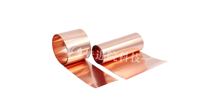
4、 Detailed explanation of the six major plating schemes
Advanced Institute Technology provides PEEK filmNickel plating, copper plating, gold plating, silver plating, titanium plating, chrome platingSix major coating schemes, each corresponding to different application scenarios:
1. Copper plating (Cu) - high conductivity, low cost
Copper has excellent conductivity and good processability. Copper plated PEEK film can be used for 5G communication substrates, millimeter wave antennas, and flexible circuits, and its low dielectric loss characteristics help reduce high-frequency signal transmission delay. Advanced Institute Technology adopts vacuum sputtering technology for copper plating, ensuring that copper atoms are evenly distributed on the surface of the film, avoiding problems such as uneven thickness and local accumulation. Copper plated PEEK is also suitable for applications that require lightweight, high temperature resistance, surface conductivity, and electromagnetic shielding.
2. Gold plating (Au) - high frequency, high reliability
Gold has extremely high chemical stability, excellent conductivity, and low contact resistance, making it the preferred choice for high-frequency and high reliability applications. Gold plated PEEK film can be used for high-frequency signal transmission, aerospace connectors, neural stimulation electrodes, and bioelectric signal acquisition. Advanced Institute of Technology adoptsCyanide free gold platingTechnology achieves high-quality gold plating while reducing environmental pollution and improving operational safety.
3. Silver plating (Ag) - efficient electromagnetic shielding
Silver is one of the most conductive metals. Silver plated PEEK film can be used to enhance electromagnetic shielding effect and is widely used in fields such as aerospace thermal control, 5G antennas, medical catheters, and special cables.
4. Nickel plating (Ni) - wear-resistant and corrosion-resistant
Chemical nickel plating (Ni-P alloy) is considered a standard process due to its mature technology and uniform coating. The nickel plating layer not only endows PEEK film with conductivity, but also serves as a bottom layer for subsequent electroplating. PPS nickel plated film electrodes have good wear resistance, corrosion resistance, and electromagnetic shielding performance.
5. Titanium (Ti) plating - biocompatibility, bone integration
Titanium coating has good biocompatibility. By depositing titanium coating on the surface of PEEK implants through plasma sputtering, the bone integration ability can be improved, making it suitable for orthopedic implant devices such as intervertebral fusion devices.
6. Chromium plating (Cr) - wear-resistant and decorative
Chromium plating has high hardness and good wear resistance, making it suitable for applications that require wear-resistant surfaces and decorative appearances.
5、 Application scenarios
Metal coated PEEK film has been practically applied in multiple high-end fields:
- 5G/6G high-frequency communication:Copper or gold plated PEEK film is used for communication substrates, antennas, and flexible circuits. The low dielectric loss characteristics of PEEK film can significantly reduce the delay and energy loss in high-frequency signal transmission.
- Aerospace:Integrating functional metal patterns on the surface of PEEK skin material can effectively enhance the integration and perception capabilities of smart skin antennas. Nickel plated or copper plated PEEK film is used as an electromagnetic shielding material to replace traditional metal components, achieving lightweight while meeting electromagnetic compatibility requirements.
- Medical devices and brain computer interfaces:PEEK films coated with gold or platinum can be used for cutting-edge biomedical applications such as neural probes and brain computer interfaces. PEEK material, with its electrically neutral properties (non-conductive, non-conductive, biocompatible), has become an ideal carrier for brain computer interface devices.
- Electromagnetic shielding:Copper plated PEEK is suitable for applications that require lightweight, high temperature resistance, surface conductivity, and electromagnetic shielding.
6、 Qualification certification and quality standards
Advanced Institute Technology has passed the following qualification certifications:
- ISO 9001Quality Management System Certification
- GJB 773ACompliant with aerospace related standards
- RoHSEnvironmental certification
National StandardGB/T 43763-2024 "Aerospace functional coatings - Special non-metallic materials - Metal coatings"It has been officially implemented, and it is clearly stipulated that various metal coatings such as nickel gold, nickel silver, copper nickel gold, etc. can be prepared on the surface of special non-metallic materials such as PEEK using electroplating or chemical plating methods. The product solution of Advanced Institute Technology strictly follows the technical requirements of the national standard.
7、 Contact Us
Advanced Institute (Shenzhen) Technology Co., Ltd. is committed to providing reliable PEEK film metallization solutions for high-end fields such as 5G communication, aerospace, and medical equipment.
Customized Hotline:0755-22277778
mobile phone13826586185 (Mr. Duan)
Fax0755-22277776
Email:duanlian@xianjinyuan.cn
Address:8th Floor, Zhongxing Building, Xinsha Road, Xinqiao Street, Bao'an District, Shenzhen
Advanced Institute (Shenzhen) Technology Co., Ltd. All rights reserved
 en
en  Español
 Français
 Português



