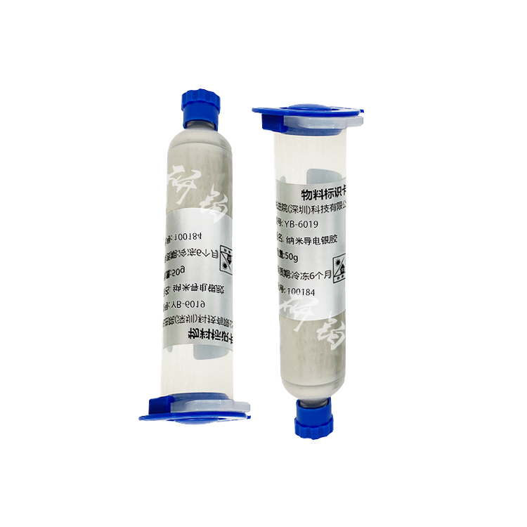
In today's rapidly evolving electronic components towards miniaturization and high density, traditional conductive materials are no longer able to meet the stringent requirements of advanced packaging processes for conductivity, thermal management capabilities, and process compatibility.Advanced Institute of TechnologyThe research platinum brand YB6019 nano conductive silver adhesive launched is reshaping the material standards in the field of electronic packaging with its breakthrough nanoscale silver particle dispersion technology, ultra-low volume resistivity, and rapid curing characteristics. This article will analyze the innovative value of this product from three dimensions: technical principles, performance breakthroughs, and application scenarios.
1、 Nano silver particles: a micro revolution in reconstructing conductive networks
The core breakthrough of YB6019 lies in its use of nanoscale silver particle dispersion technology. Traditional conductive silver paste relies on micron sized silver powder to construct conductive pathways, but the contact area between particles is limited, resulting in a volume resistivity generally in the range of 10 ⁻³ to 10 ⁻Ω· cm. YB6019, through the synergistic optimization of chemical reduction method and mechanical ball milling process, controls the silver particle size within the range of 20-50 nanometers, with a particle size distribution standard deviation (CV value) of less than 8%. This ultrafine particle has a huge specific surface area and forms a conductive network of "point contact surface coverage" in the resin matrix, reducing the volume resistivity to 8 × 10 ⁻⁶Ω· cm, which is two orders of magnitude higher than traditional products.
A well-known enterprise in Jiangxi Province found in practical applications that using YB6019 packaged Mini LED chips, the contact resistance between the chip and the substrate is reduced by 63% and the light efficiency is improved by 8% compared to traditional silver paste under a driving current of 100mA. This is due to the "sintered neck" structure formed by nano silver particles during the solidification process - adjacent particles achieve metallurgical bonding through surface diffusion, forming conductive channels close to bulk silver. Scanning electron microscopy (SEM) observations show that the porosity of the silver layer after solidification of YB6019 is less than 3%, far below the industry average of 8% -12%.
2、 Fast curing: solving the dual challenges of production efficiency and reliability
The demand for curing speed in electronic packaging technology is becoming increasingly stringent. Traditional epoxy resin based conductive silver adhesive needs to be cured at 150 ℃ for 30 minutes, which not only limits the production line pace but may also cause chip warping due to thermal stress. YB6019 achieved a rapid curing process at 120 ℃/5 minutes by optimizing the organic carrier formula, using modified acrylic ester as the matrix resin, and combining it with an efficient latent curing agent.
3、 Multi scenario adaptation: full coverage from consumer electronics to high-end power devices
YB6019 Nano Conductive Silver AdhesiveThe breakthrough is not only reflected in performance indicators, but also in its deep adaptation to diverse application scenarios. In the field of consumer electronics, Jiangxi enterprises apply it to the electromagnetic shielding layer connection of flexible circuit boards (FPC). The flexibility of nano silver particles enables the adhesive layer to undergo 5000 bending cycles at a bending radius of 5mm, with a resistance change rate of less than 5%, meeting the dynamic reliability requirements of wearable devices.
In the high-end power device market, YB6019 is gradually replacing traditional sintered silver paste. A certain automotive electronics company uses YB6019 packaged SiC MOSFET modules. Actual testing shows that under high temperature service conditions of 175 ℃, the contact resistance of the module remains stable below 0.2m Ω, which is 15% lower than that of sintered silver paste; At the same time, due to the absence of high-pressure sintering equipment, the investment cost of a single production line is saved by about 3 million yuan. The characteristics of "low-temperature sintering and high-temperature service" make YB6019 an ideal solution for third-generation semiconductor packaging.
4、 Technological Extension: The Future Evolutionary Direction of Nano Silver Adhesive
The success of YB6019 is not the end point, but the starting point of the iteration of nano conductive silver paste technology. The R&D team of the Advanced Institute of Technology has revealed that the next generation of products will focus on developing a light curing system to further shorten the curing time to less than 10 seconds, meeting the needs of ultra-thin chip packaging. In addition, in the field of bioelectronics, the team is exploring nano silver gel formulations with biocompatibility, which may be applied to implantable medical devices in the future.
The practice of Jiangxi enterprises shows that,Nano conductive silver adhesiveIt has moved from laboratory to large-scale application, and its value is not only reflected in performance improvement, but also in providing a more efficient and reliable connection solution for the electronic packaging industry. With the rise of domestic high-end products such as YB6019, the independent and controllable ability of Chinese enterprises in the field of electronic materials is significantly enhanced, which may be the most profound significance of this materials revolution.

 en
en  Español
 Français
 Português



