Nano copper pasteLighting up the future light of LED packaging
In today's rapidly advancing technology, LED (Light Emitting Diode), as the core of the new generation of lighting technology, is changing our lives at an unprecedented speed. From home lighting to urban night scenes, from mobile phone screens to large display screens, LED has become a shining star in the field of lighting and display due to its high efficiency, energy saving, long lifespan, environmental protection and other characteristics. However, behind this, a key material innovation is silently driving the leap of LED technology - that isAdvanced Institute of TechnologyInnovative application of self-developed nano copper paste in LED packaging.
1、 Nano copper paste: integration of technology and art
Nano copper paste, as the name suggests, is a paste made by processing copper powder to the nanometer level and mixing it with a specific organic carrier. This seemingly simple material actually contains enormous technological content and artistic beauty. Nano level copper powder, due to its unique physical and chemical properties such as extremely high specific surface area, excellent conductivity, and good thermal conductivity, has brought revolutionary changes to LED packaging.
2、 The Revolution of Encapsulation Efficiency: A Leap from Theory to Practice
During the LED packaging process,Micro scale conductive copper pasteIts main function is to serve as a bridge for conductivity and thermal conduction, connecting LED chips with external circuits, while effectively dissipating heat and ensuring the long-term stable operation of LEDs. Traditional packaging materials often face problems such as insufficient conductivity, high thermal resistance, and complex packaging processes, which limit the improvement of LED performance. The introduction of nano copper paste is like injecting a shot in the arm into LED packaging.
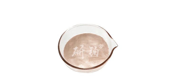
1. Leap in conductivity: Copper powder in nano copper paste can form a more compact and uniform conductive network due to its small size effect, significantly improving current transmission efficiency, reducing energy consumption, and making LED light emission brighter and more uniform.
2. Thermal management optimization: Efficient thermal conductivity is another highlight of nano copper paste. The large amount of heat generated during the operation of LED can be quickly conducted to the outside of the package, effectively preventing chip overheating and extending the service life of LED.
3. Simplify packaging process: The good fluidity and adhesion of nano copper paste make the packaging process more flexible and efficient, reduce production costs, and improve production efficiency.
3、 Catalyst for green lighting: dual guarantee of environmental protection and efficiency
With the increasing global awareness of environmental protection, green and low-carbon have become the key words for the development of the LED industry.Printed copper paste for circuit boardsThe application of LED not only improves the performance of LED, but also promotes the environmental transformation of the entire industry chain. Compared to traditional packaging materials, nano copper paste has a smaller impact on the environment during production and use, which is in line with the concept of sustainable development. Meanwhile, its efficient energy conversion rate makes LED lighting more energy-efficient, contributing technological strength to reducing carbon emissions and addressing climate change.
4、 Looking ahead to the future: Nano copper paste leads the new era of LED packaging
Looking ahead to the future, with the continuous advancement of nanotechnology and materials science, the application prospects of nano copper paste in LED packaging will be even broader. On the one hand, researchers will continue to explore more possibilities of nano copper paste, such as further improving its conductivity and thermal conductivity through surface modification technology, or developing composite nano copper paste with specific functions to meet the needs of different application scenarios. On the other hand, with the development of intelligent manufacturing and automation technology, the packaging process of nano copper paste will become more intelligent and precise, promoting the LED industry to move towards a higher level.
In short,Conductive ink for LED circuit boardAs an important achievement of advanced technology, it is illuminating the future path of LED packaging technology with tangible performance improvements and environmental contributions. It is not only a technological innovation, but also a brave attempt by humanity to pursue a more efficient and environmentally friendly lifestyle. In this era of intertwined light and shadow, nano copper paste is working hand in hand with LED to create beautiful pictures of light and hope.

 en
en  Español
 Français
 Português



