Innovating the Future: Exploring PCB Rapid DevelopmentPrinting copper pasteThe Revolutionary Road of Craftsmanship
In today's rapidly advancing technology, the iteration speed of electronic products is astonishing. As the heart of electronic devices, the production process of electronic circuit boards (PCBs) is constantly pursuing more efficient, precise, and environmentally friendly solutions. In this context, the Advanced Institute, with its profound accumulation in the fields of materials science and electronic engineering, has successfully developed a revolutionary PCB rapid printing copper paste process, bringing unprecedented changes to the PCB manufacturing industry.
1、 The limitations and challenges of traditional craftsmanship
In traditional PCB manufacturing processes, copper foil etching is the mainstream method. Although this method is technically mature, it has problems such as large material waste, long production cycles, and serious environmental pollution. Especially when facing complex circuit patterns and high-precision requirements, the limitations of etching methods become increasingly apparent. Moreover, with the rapid development of emerging fields such as 5G, the Internet of Things, and wearable devices, the demand for flexibility and customization of PCBs is increasing. Traditional processes are no longer able to meet the urgent needs of the market for rapid response and low-cost production.
2、 PCB rapid printing copper paste process: a quiet revolution
In response to the above challenges,Advanced InstituteAfter countless experiments and optimizations, the research team has finally developed this PCB rapid printing copper paste process. The core of this process lies in the combination of innovative copper paste formula and high-precision printing technology, which realizes the direct conversion from design to finished product, greatly shortens the production cycle, reduces costs, and reduces environmental pollution.
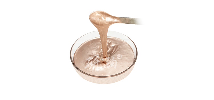
1. Copper paste innovation: The formula of copper paste is the key to this technology. By optimizing the particle size distribution of copper powder and adding special additives, the copper slurry has good fluidity and adhesion, and can achieve uniform and dense deposition on various substrates. This not only improves the conductivity of the circuit, but also ensures high-precision replication of the circuit pattern.
2. High precision printing technology: Advanced inkjet printing or screen printing technology, combined with computer-aided design systems, can accurately control the deposition position and thickness of copper paste, achieving one-time molding of complex circuit patterns. This' what you see is what you get 'production method greatly simplifies the production process and improves production efficiency.
3、 Dual leap in production efficiency and environmental protection
PCB rapid printing copper pasteThe application of technology marks a qualitative leap in the production efficiency of PCB manufacturing industry. Compared to traditional etching methods, the new process has shortened the production cycle by more than 30%, significantly improved material utilization, and greatly reduced waste emissions. This not only reduces production costs, but also conforms to the current global trend of green and low-carbon development, injecting new vitality into the sustainable development of enterprises.
4、 Embark on a new chapter of customization and flexible production
More importantly, this process has opened up a new path for customized production of PCBs. Whether it is flexible circuit boards in small wearable devices or high-density interconnect boards in large servers, efficient and precise manufacturing can be achieved through fast printing copper paste technology. This flexibility not only meets the market's demand for diversified products, but also provides designers with greater creative space, accelerating the speed of new product launches.
Conclusion: Looking into the future, infinite possibilities
Advanced Institute's PCB Rapid DevelopmentCopper conductive pasteCraftsmanship is not only a technological innovation in the field of PCB manufacturing, but also a forward-looking layout for the future era of intelligent electronics. It not only solves many pain points in traditional craftsmanship, but also brings new growth points and development opportunities to the industry. With the continuous maturity and popularization of technology, we have reason to believe that this quiet revolution will lead the PCB manufacturing industry towards a more efficient, environmentally friendly, and flexible new era, providing strong support for technological innovation and industrial upgrading. On the path of exploring the future, Advanced Institute works hand in hand with every colleague to create brilliance.

 en
en  Español
 Français
 Português



