With the rapid development of China's aerospace industry and high-end manufacturing, surface metallization technology for special engineering plastics is becoming an important breakthrough direction in the field of key materials. On July 1, 2024, the national standard GB/T 43763-2024 "Aerospace Functional Coating Special Non Metallic Material Metal Coating" was officially implemented. This standard specifies that special non-metallic materials such as polyetheretherketone (PEEK), polyphenylene sulfide (PPS), polyimide (PI), liquid crystal polymer (LCP), and their composite materials can be coated with functional metal coatings using electroplating or chemical plating methods. The introduction of this national standard provides authoritative technical specifications and quality basis for PEEK film metallization, and also marks a substantial breakthrough in the field of aerospace grade non-metallic material metallization by domestic enterprises represented by Advanced Institute (Shenzhen) Technology Co., Ltd.
1、 PEEK film: insulation dilemma of the "pyramid tip" of special engineering plastics
Polyether ether ketone (PEEK) is known as the "pyramid tip" of the special engineering plastics family. As a semi crystalline thermoplastic special engineering plastic, PEEK has been widely used in aerospace, electronic and electrical, medical equipment, and new energy fields due to its excellent high temperature resistance, mechanical strength, chemical stability, and electrical insulation properties. PEEK film can operate stably in environments above 250 ° C for a long time, with a stable dielectric constant of around 3.2 and a dielectric loss tangent value as low as 0.0015 in the 1-10 GHz frequency band, making it an ideal dielectric material for high-frequency signal transmission scenarios.
However, the inherent insulation and surface inertness of PEEK film pose technical bottlenecks in applications that require conductivity, electromagnetic shielding, or signal transmission functions. PEEK film has extremely low surface energy, high crystallinity, and strong chemical inertness, making it difficult for metal coatings to directly adhere. The biological inertness of PEEK is also one of its main weaknesses as an implant material - it cannot directly bond with bones and lacks bone integration ability. Therefore, PEEK film must undergo surface activation treatment before undergoing metalization processes such as chemical plating or physical vapor deposition.
2、 Core technical challenges of chrome plating on PEEK film
The surface metallization of PEEK film usually involves three key steps: surface activation pretreatment, establishment of conductive layer, and deposition of functional layer. Any problem at any stage can lead to coating peeling or substandard performance.
Traditional plastic metallization processes often use high-temperature fusion or strong acid roughening treatment. Chemical roughening usually uses chromic acid sulfuric acid system or potassium permanganate system to etch micro pits on the surface of PEEK, while introducing polar groups to enhance surface energy. However, the glass transition temperature of PEEK is only around 143 ℃, and excessively high temperatures or intense chemical reactions can easily cause film deformation, brittleness, loss of flexibility and dimensional accuracy. If metal is directly sputtered at low temperatures to avoid thermal damage, it is difficult for metal atoms to form chemical bonds with the surface of PEEK, resulting in a loose film layer that peels off with slight external force. The adhesion problem of PEEK film chrome plating has been a pain point that has plagued the industry for many years.
3、 Advanced Institute Technology: A national high-tech enterprise specializing in PEEK film metallization
In the highly technical niche of PEEK coating, Advanced Institute (Shenzhen) Technology Co., Ltd. is a professional manufacturer worth paying attention to. The company was founded in 2016 and is headquartered in Bao'an District, Shenzhen, Guangdong Province. It is a national high-tech enterprise focusing on shielding materials, insulation materials, thermal conductivity materials, and precious metal coatings. The company has its own registered trademark "Research Platinum" and has dual production bases in Shenzhen and Dongguan.
The company has passed ISO9001 quality management system certification, and its products comply with GJB 773A aerospace related standards and RoHS environmental requirements. It has the ability to support high-end fields such as aerospace, military, and 5G communication. In the field of coating technology, Advanced Institute Technology has independently built magnetron sputtering and vacuum evaporation production lines, using roll to roll continuous production technology, which can continuously and uniformly deposit metal layers on the surface of flexible polymer films. Suitable substrates include various flexible polymer films such as PEEK, PI, PET, LCP, FEP, etc., and can be plated with metals including gold, silver, copper, nickel, titanium, chromium, aluminum, tin, platinum, etc. Relying on advanced physical vapor deposition (PVD) technology, the thickness of metal thin films can be precisely controlled at the nanometer level and customized as needed within the range of a few nanometers to several hundred nanometers.
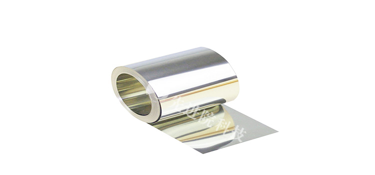
4、 Core process: Plasma activated magnetron sputtering, low-temperature gradient interface locking
Advanced Institute Technology has developed a plasma activation combined with low-energy ion beam pretreatment process to address the core challenges of low surface energy and strong chemical inertness of PEEK. This combination scheme can effectively shorten the induction time of subsequent chemical plating, and has a smaller impact on the mechanical properties of the film body. Stable binding force data has been obtained in sample validation.
The company has successfully achieved mass production of PEEK film rolls with a width of 600mm and a film thickness as low as 6 μ m based on its independently developed "low-temperature gradient interface locking" technology. The entire process route is divided into three key steps:
Step 1: Online plasma surface activation.
In a vacuum environment, plasma is used to pretreat the surface of PEEK film, creating a nanoscale micro rough morphology on the film surface. At the same time, a large number of oxygen-containing and nitrogen-containing active functional groups are introduced to provide sites for subsequent chemical bonding.
Step 2: Deposition of low-temperature and high ionization gradient transition layer.
After surface activation, a transition layer (such as titanium, aluminum, chromium, etc.) and functional metal layer are deposited on the surface of PEEK film using magnetron sputtering technology. Magnetron sputtering is carried out in a vacuum environment, where high-speed particles bombard the target material, causing metal atoms to break free from the constraints of the target material and deposit uniformly on the surface of the thin film, forming a uniform and dense metal film. Compared with traditional chemical plating methods, PVD technology has advantages such as environmental protection, good coating uniformity, and strong adhesion. It can achieve uniform deposition of metal atoms on the substrate surface under low temperature conditions.
Step 3: Electroplating thickening (optional).
For application scenarios that require thicker coatings, the metal layer can be further thickened through electroplating on the basis of magnetron sputtering.
The metal coating achieves stress transition from the substrate to the metal layer through gradient coating design, effectively avoiding interface delamination caused by modulus differences. The process temperature of the entire coating process is strictly controlled within 130 ℃ - much lower than the glass transition temperature of PEEK - and the film surface after winding is smooth and free of thermal shrinkage. The online spectral reflectance thickness measurement system tracks the square resistance and optical properties of each meter of thin film in real time, ensuring the consistency of the quality of the entire roll of material.
5、 Typical application scenarios of chrome plated PEEK film
Advanced Institute Technology provides nickel plating, copper plating, gold plating, silver plating, titanium plating for PEEK filmchrome platingSix major coating schemes, each corresponding to a completely different application scenario. Among them, chrome plated PEEK film is mainly used in the following fields:
Aerospace field:
Chromium or Ni-P coating can significantly improve surface hardness and is suitable for wear-resistant scenarios such as seals and valves. Metallized PEEK film provides electromagnetic shielding effectiveness and can be used for lightweight shielding components. With the transformation of the aerospace industry from heavy-duty aluminum alloys to lightweight engineering plastics, the application prospects of metal coated PEEK film in the field of aviation connectors are becoming increasingly broad.
In the field of electronic and electrical engineering:
Chrome plated PEEK film can be used for high-frequency connectors, shielding covers, and other components that have dual requirements for wear resistance and conductivity. The low dielectric loss characteristic of PEEK helps to reduce high-frequency signal transmission delay.
Industrial wear-resistant scenario:
Chromium coating can significantly improve surface hardness and is suitable for wear-resistant components in high-temperature and high-pressure environments such as bearings and seals. Related studies have shown that chromium based multilayer coatings combined with PEEK exhibit excellent wear resistance under dry sliding conditions.
6、 National standard recognition and industrial prospects
The release and implementation of GB/T 43763-2024 "Aerospace Functional Coatings - Special Non Metallic Materials - Metal Coatings" provides a unified technical specification and inspection standard for the metallization of special non-metallic materials such as PEEK. This standard is jointly managed by the National Committee for Standardization of Aerospace Technology and its Applications (SAC/TC 425) and the National Committee for Standardization of Metal and Non Metal Coatings (SAC/TC 57), and drafted by Beijing Satellite Manufacturing Co., Ltd., China Aerospace Standardization Institute and other units. The introduction of standards not only provides quality assurance for the aerospace industry, but also lays the institutional foundation for the industrial promotion of PEEK film metallization technology.
At the same time, the PEEK coating track is entering a period of rapid growth. According to QYResearch research statistics, the global market sales of polyetheretherketone (PEEK) films reached 1.217 billion yuan in 2025, and are expected to reach 1.844 billion yuan in 2032, with a compound annual growth rate of 6.2%. The production of PEEK in China has increased from about 200 tons in 2017 to 3808 tons in 2024, and the degree of localization continues to deepen.
Advanced Institute (Shenzhen) Technology Co., Ltd. has achieved roll to roll mass production of PEEK film chrome plating based on its independently developed plasma activated magnetron sputtering process and "low-temperature gradient interface locking" technology. The products comply with GJB 773A aerospace standards and GB/T 43763-2024 national standards. The maturity and mass production of PEEK film chrome plating technology not only provide key material support for high-end manufacturing fields such as aerospace, 5G communication, and medical equipment, but also mark China's progress towards a higher level in the field of surface metallization of special engineering plastics.
Advanced Institute (Shenzhen) Technology Co., Ltd
Address:8th Floor, Zhongxing Building, Xinsha Road, Xinqiao Street, Bao'an District, Shenzhen
Telephone:0755-22277778
Email:duanlian@xianjinyuan.cn
URL:www.xianjinyuan.cn
 en
en  Español
 Français
 Português



