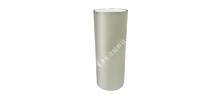
Under the development trend of miniaturization of electronic components, precision of optical equipment, and high reliability of medical devices, breakthroughs in material properties have become the core driving force for industry upgrading. Advanced Institute of Technology's research and development and mass productionNickel plating on 25 μ m PP filmThe product, with its excellent conductivity, corrosion resistance, and process stability, has become a key foundational material in the fields of electronics, optics, and healthcare, providing reliable technical support for high-end manufacturing.
Dual conductivity and corrosion resistancebreakthrough
PP (polypropylene) film itself has excellent insulation properties, but through the nickel plating process independently developed by advanced institute technology, a uniform and dense metal nickel layer is formed on the surface of the film, achieving a qualitative leap in its conductivity. Experimental data shows that the surface resistivity of the product is as low as 10 Ω· cm, fully meeting the stringent requirements for conductive materials in high-frequency circuits, electromagnetic shielding, and other scenarios. At the same time, as an inert metal, the nickel layer performs well in corrosive environments such as salt spray and acid alkali. After 72 hours of neutral salt spray testing, the surface of the film is free of oxidation and detachment, ensuring long-term reliability. This dual performance fusion makes nickel plating on 25 μ m PP film an ideal choice in electronic packaging, flexible circuit substrates, and other scenarios.
Technological innovation empowers product stability
Advanced Institute of TechnologyBy adopting a composite process of chemical plating and electroplating, and precisely controlling parameters such as plating solution composition, temperature, and current density, the industry leading level of nickel layer thickness uniformity error less than ± 0.1 μ m has been achieved. This technological breakthrough not only avoids the edge effect that traditional coatings are prone to, but also significantly improves the flexibility of the film - even after 100000 bending tests, the coating remains intact without cracks or peeling. In addition, the entire process uses environmentally friendly plating solution, without harmful substances such as hexavalent chromium, and complies with international environmental standards such as RoHS and REACH, providing safety guarantees for medical grade applications.
Multi domain application verification performance advantages
In the field of electronics, a well-known communication company has applied this product to 5G base station filter components, utilizing its high conductivity to reduce signal loss, while extending the outdoor service life of the equipment through its corrosion resistance, and extending the maintenance cycle to more than 5 years. In the field of optics, a precision instrument manufacturer uses nickel plated PP film as the substrate for laser reflectors. The combination of low thermal expansion coefficient (≤ 5 × 10 ⁻⁶/℃) and high thermal conductivity (≥ 20 W/m · K) effectively improves the stability and energy efficiency of laser equipment. In the medical field, a certain implantable device company used the material for the insulation layer of nerve stimulation electrodes after strict biocompatibility testing. Its resistance to body fluid corrosion ensures the long-term safe operation of the device in the human body.
Customized services meet differentiated needs
Advanced Institute Technology provides multi thickness coating options from 0.5 μ m to 5 μ m, and supports customized production of parameters such as film width and roll diameter. A well-known electronics company in Guangzhou initially only purchased small batches of samples for reliability testing, including 12 rigorous tests such as high temperature and high humidity (85 ℃/85% RH) storage and mechanical impact. After confirming that the product performance fully meets the standards, the company listed Advanced Institute Technology as a strategic supplier.
Environmental protection and energy conservation lead industry upgrading
Compared to traditional vacuum coating processes, Advanced Institute Technology's wet nickel plating technology reduces energy consumption by 40%, and the recycling rate of the plating solution exceeds 95%, significantly reducing carbon emissions during the production process. This advantage makes it the preferred material solution for export-oriented enterprises in the context of EU carbon tariffs and other policies. At present, the product has passed international certifications such as UL and T Ü V, and serves customers in more than 20 countries and regions around the world.
From laboratory research and development to large-scale production, Advanced Institute Technology has redefined the functional boundaries of PP films through technological innovation.Nickel plating on 25 μ m PP filmIt is not only a material, but also a bridge connecting basic research and industrial applications. Its performance stability and process environmental friendliness are continuously driving the development of electronics, optics, and medical fields towards higher precision and longer lifespan.

 en
en  Español
 Français
 Português



