PI Nickel and Copper Plating: Innovative Leap of Advanced Institute Technology
In today's rapidly advancing high-tech world, every breakthrough in materials science has the potential to lead an industrial revolution. Shenzhen Advanced Institute Technology Co., Ltd., as a leader in the field of new materials, is embarking on a journey of expanding material properties and application boundaries with PI (polyimide) nickel and copper plating technology as its core. This technology not only combines the excellent performance of polyimide with the conductive and protective properties of metal coatings, but also represents the crystallization of advanced scientific and technological wisdom and innovative spirit.
1、 PI material: the foundation of excellent performance
Polyimide, known as the "golden film" material, occupies a place in many high-tech fields due to its excellent high temperature resistance, chemical corrosion resistance, good mechanical strength, and electrical insulation performance. From aerospace to microelectronic packaging, the application of PI materials is ubiquitous, showcasing their unique charm as high-performance materials. However, a single PI material is difficult to meet the needs of all application scenarios, especially when good conductivity or specific protective properties are required. The birth of PI nickel and copper plating technology undoubtedly provides an elegant solution to this problem.
2、 Nickel plating and copper plating: integration of technology and art
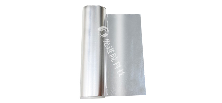
In the laboratory of advanced technology, researchers have successfully deposited one or more layers of nickel and copper uniformly on PI substrates through precise chemical and physical processes. This process may seem simple, but it actually involves countless experiments and optimizations, and is a comprehensive application of interdisciplinary knowledge such as materials science, electrochemistry, and surface engineering. The nickel plating layer endows the material with excellent corrosion resistance and a certain degree of hardness, while the copper plating layer further enhances conductivity while reducing costs. This' strong alliance 'makesPI nickel plated copper plated materialOn the basis of maintaining the original PI characteristics, it has a wider range of application potential.
3、 Innovative applications: unlocking infinite possibilities
With the rapid development of emerging fields such as 5G communication, flexible electronics, and wearable devices, the requirements for materials are becoming increasingly stringent. PI nickel and copper plated materials have become an ideal choice in these fields due to their lightweight, high strength, good weather resistance, and excellent electromagnetic shielding performance. In 5G antenna design, it can effectively improve signal transmission efficiency and reduce signal interference; In the manufacturing of flexible display screens, their flexibility and conductivity provide a solid material foundation for the bending and folding of the screen; On wearable devices, PI nickel plated copper plated material not only ensures the durability of the device, but also enhances the user experience by optimizing electromagnetic compatibility.
4、 Environmental Protection Concept: Practitioners of Green Production
While pursuing technological innovation,Advanced Institute of TechnologyAlways remember the responsibility towards the environment. The production process of PI nickel and copper plating strictly follows environmental standards, using low pollution and high-efficiency plating solution formulas to reduce the emission of harmful substances. In addition, through recycling and waste management strategies, the sustainability of production activities is ensured, demonstrating the beauty of the balance between technological innovation and green development for enterprises.
5、 Looking to the future: continuous exploration, continuous progress
Facing the future, Advanced Institute Technology is well aware that,PI nickel and copper plating technologyThe potential goes far beyond that. With the continuous advancement of materials science, nanotechnology, and intelligent manufacturing, the performance of PI nickel plated copper plated materials will be further optimized, and their application fields will become more extensive. The company is increasing its research and development investment, exploring the integration of PI composite materials with more advanced technologies such as graphene reinforcement and intelligent responsiveness, aiming to provide more diversified and high-performance material solutions for global customers.
In the innovative journey of advanced technology, PI nickel and copper plating technology is not only a symbol of technological progress, but also a reflection of the responsible attitude of enterprises towards society and the environment. It is like a beam of light, illuminating the path of material science exploration and leading the industry towards a more intelligent, green, and efficient future.

 en
en  Español
 Français
 Português



