PI Copper Coating: An Important Driver for Opening the Era of High Performance Electronic Materials
1、 Core foundational materials for high-performance electronic devices
Advanced Institute (Shenzhen) Technology Co., LtdThe PI copper plated film has become an ideal substrate for flexible circuit boards (FPCB), chip packaging, and high-frequency electronic devices due to its excellent high temperature resistance, mechanical strength, and chemical stability. The combination of the conductivity of copper layer and the insulation of PI achieves a balance between high-speed signal transmission and reliable insulation, meeting the ultimate requirements for material performance in 5G communication, artificial intelligence hardware, and other fields.
2、 Promote the revolution of flexible electronic technology
The lightweight and flexible properties of PI copper plated film make it a key material for foldable smartphones and wearable devices. For example, the driving circuit of flexible OLED screens relies on the bending durability of PI copper plated films, breaking through the physical limitations of traditional rigid circuits and promoting innovation in consumer electronics forms.
3、 Improve the transmission efficiency of high-frequency signals
In high-frequency millimeter wave applications such as autonomous driving radar and satellite communication,PI copper foilThe dielectric loss is extremely low, and the high purity of the copper layer can reduce signal attenuation. This characteristic enables electronic devices to maintain stability at higher frequencies, directly supporting the development of the Internet of Things and high-speed data exchange technology.
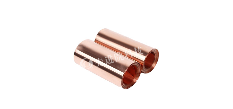
4、 Strengthen the reliability of extreme environments
Aerospace, new energy vehicles and other fields require materials to work in high-temperature, high humidity or vibration environments for a long time. The temperature resistance range of PI substrate (-269 ℃~400 ℃) combined with the anti-oxidation coating technology of copper layer significantly improves the service life of electronic components under complex working conditions and reduces the system failure rate.
5、 Promote the trend of green manufacturing and miniaturization
Advanced Institute of TechnologyPI copper plated filmMicro level circuit patterns can be achieved through precision etching technology, reducing material waste; Its lightweight characteristics (reducing weight by more than 70% compared to traditional glass fiber substrates) meet energy-saving requirements. Meanwhile, the ultra-thin structure (up to 8 μ m) provides the possibility for miniaturization of electronic devices, accelerating the landing of cutting-edge applications such as medical implants.
6、 Catalyst for upgrading the industrial chain
Polyimide copper-clad laminateThe technological barriers are driving the iteration of upstream PI resin synthesis and precision electroplating processes, while downstream industries such as semiconductor packaging and display panels are upgrading. The partial technological breakthroughs of Chinese enterprises, such as the mass production of domestically produced PI films, are gradually changing the pattern of relying on imported high-end materials.
Conclusion
The PI copper plating film of Advanced Institute Technology is not only an advancement in a single material, but also redefines the performance boundaries of electronic materials through interdisciplinary collaborative innovation. With the increasing demand for ultra-thin and highly conductive materials in cutting-edge fields such as quantum computing and brain computer interfaces, their strategic value will continue to be released, becoming a fundamental pillar of the future electronics industry.

 en
en  Español
 Français
 Português



