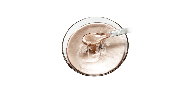
PCB through-hole copper pasteHigh adhesion prevents the copper layer through the hole from falling off
Introduction
In the manufacturing of printed circuit boards, through holes are a key structure for achieving electrical connections between different layers of circuits. If the adhesion of the through-hole copper layer is insufficient, it is prone to detachment or fracture under thermal stress, mechanical stress, or long-term use, leading to the failure of the entire board. Therefore, ensuring high adhesion between the through-hole copper layer and the substrate (usually resin and glass fiber) is the core of ensuring PCB reliability.Advanced Institute (Shenzhen) Technology Co., LtdCopper paste, as a key material, plays a decisive role in its characteristics and process.
1、 Microscopic bite between copper paste and pore wall
This is the physical basis for forming adhesion. The walls of PCB drilling holes are not absolutely smooth, but have slight unevenness. The solid copper particle morphology and particle size distribution in the formula of high-performance copper paste are carefully designed to effectively penetrate and 'anchor' in these microscopic rough structures. This mechanical interlocking effect is like countless small hooks, firmly fixing the copper layer to the hole wall and serving as the first line of defense against detachment.
2、 Chemical fusion of resin system and substrate
This is the chemical key to achieving high adhesion. Copper paste is not pure metal powder, it contains a special organic resin system. This resin must have excellent compatibility and reactivity, and be able to interact or covalently bond with the resin material of the PCB substrate itself (such as epoxy resin). In the subsequent curing process, the two blend together and form a strong chemical bond at the interface, thereby tightly "bonding" the copper layer and substrate together, greatly enhancing the bonding strength.
3、 Volume control and internal stress elimination during the curing process
Curing is the process by which copper paste transforms from a paste into a sturdy conductor. If the shrinkage rate is too large during the curing process, a huge internal stress will be generated, and this "tensile stress" will attempt to peel off the copper layer from the pore wall. High adhesion copper paste achieves smooth and uniform curing by optimizing its curing curve (temperature, time) and formula, minimizing volume shrinkage and internal stress, ensuring a dense and stable copper layer structure.
4、 Stability and durability of interface layer
The adhesion is not only strong, but also long-lasting. PCB will experience harsh environments such as high temperature and humidity during subsequent assembly and use. The interface layer formed by high-performance copper paste must have excellent heat and moisture resistance to prevent a decrease in bonding strength due to moisture absorption expansion or high-temperature degradation. A stable interface ensures effective adhesion throughout the entire lifecycle of the product.
Summary
In summary, Advanced Institute (Shenzhen) Technology Co., LtdHigh conductivity through-hole copper pasteRealizing high adhesion and preventing detachment is a systematic project. It achieves micro interlocking physically, interface fusion chemically, controls curing stress in the process, and ensures interface stability in long-term reliability. These four aspects work together to build a sturdy and durable foundation for the through-hole copper layer, thereby ensuring the overall quality and lifespan of the PCB.

 en
en  Español
 Français
 Português



