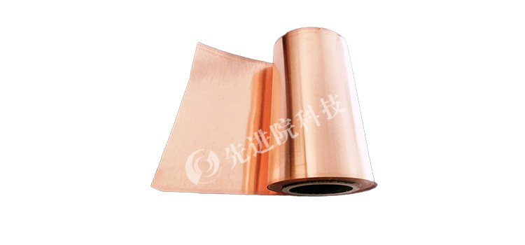
In today's era of rapid technological development, the progress of materials science is profoundly changing the landscape of many industries. PI copper plated film, as an emerging high-performance composite material, has shown great potential in many fields such as electronics, new energy, aerospace, etc. due to its unique performance advantages, and has become a focus of attention for many research institutions and enterprises. The PI copper plated film produced by Advanced Institute Technology stands out in the market with its excellent quality and advanced production technology.
Vacuum sputtering technology:PI copper plated filmThe cornerstone of quality
The PI copper plated film produced by Advanced Institute Technology is usually plated with copper using vacuum sputtering technology. This technique is like a skilled craftsman meticulously carving each layer of copper film in a vacuum environment. In a vacuum environment, copper atoms or molecules are sputtered out and uniformly deposited on the surface of a PI thin film like finely controlled particles by high-speed particle bombardment of a copper target, ultimately forming a uniform and dense copper film.
This unique process method has many significant advantages. From the perspective of coating uniformity, vacuum sputtering technology can ensure an extremely uniform distribution of copper atoms on the surface of PI thin films, avoiding problems such as uneven coating thickness and local defects that may occur with traditional coating methods. Taking the testing conducted by a physics research institute in Lanzhou as an example, the institute found that the fluctuation range of coating thickness on a sample with an area of 100cm ² did not exceed ± 0.5 μ m during strict testing of the PI copper plating film of advanced institute technology, fully demonstrating the excellent performance of this process in uniformity.
In terms of adhesion, the coating formed by vacuum sputtering technology has a strong bonding force with the PI film, reaching a level of 5B. This means that after a series of rigorous adhesion tests, there is almost no peeling phenomenon between the coating and the substrate. In practical applications, this strong adhesion can ensure that the PI copper plating film can maintain stable performance in various complex environments, without affecting the quality and reliability of the product due to coating detachment.
At the same time, this technology can also maintain the excellent performance of PI film. The PI film itself has the characteristics of high temperature resistance, good insulation, and high mechanical strength, and the vacuum sputtering copper plating process adds new properties such as conductivity to it without affecting these properties, achieving optimization and expansion of performance.
Multi dimensional performance advantage: meeting diverse application needs
Bending resistance: flexible response to complex working conditions
Advanced Institute of TechnologyThe PI copper plated film exhibits excellent bending resistance and has no cracks within ten cycles. This feature gives it a unique advantage in application scenarios that require frequent bending. Taking flexible electronic devices as an example, with the rise of wearable devices, foldable screen phones and other products, high requirements have been put forward for the flexibility and bending resistance of materials. The PI copper plated film can maintain the integrity of the structure during repeated bending, ensuring stable connection of the circuit and providing reliable material support for the development of flexible electronic devices.
Accurate and controllable thickness: suitable for different application scenarios
The thickness range of PI copper plating film from Advanced Institute Technology is between 5-125 μ m, and this precise controllability enables it to meet the needs of different application scenarios. In the field of microelectronics, for some precision circuit boards and chip packaging, thin copper plated films are required to achieve high-density integration and good signal transmission. The 5 μ m thin copper plating film can meet the needs of these high-end applications and provide strong support for the development of microelectronics technology.
In some fields that require high conductivity and mechanical strength, such as electrode materials for new energy batteries, thicker copper plated films can provide better conductivity and structural support. A 125 μ m thick copper plating film can increase the conductive area of the electrode, improve the charging and discharging efficiency of the battery, enhance the mechanical stability of the electrode, and extend the service life of the battery.
The choice of a physics research institute in Lanzhou: authoritative certification of quality
As a well-known research institution in China, a physics research institute in Lanzhou has profound accumulation and rich experience in materials research and application. When selecting a PI copper plating film supplier, the department conducted comprehensive and rigorous testing and evaluation. From the physical and chemical properties of materials to their actual application effects, every step has been carefully tested and analyzed.
After a series of rigorous tests, a physics research institute in Lanzhou finally decided to purchase PI copper plated film from Advanced Institute Technology for the production of its products. This choice is not only an authoritative certification for the quality of advanced scientific and technological products, but also provides important reference for other enterprises and research institutions. The relevant person in charge of the research institute stated that the PI copper plating film of Advanced Institute Technology has met or exceeded their expectations in various performance indicators, which can meet the production needs of their high-end products, and has obvious advantages in production technology and quality control.
Looking ahead to the future:PI copper plated filmThe vast prospect
With the continuous advancement of technology and the increasing demand for high-performance materials in various industries, the market prospect of PI copper plated film is very broad. In the field of electronics, with the rapid development of technologies such as 5G communication, the Internet of Things, and artificial intelligence, the demand for high-performance electronic materials will continue to grow. PI copper plated film, with its excellent conductivity, flexibility, and high temperature resistance, is expected to be widely used in high-speed circuit boards, flexible display screens, sensors, and other fields.
In the field of new energy, with the booming development of industries such as electric vehicles and energy storage batteries, the requirements for battery performance are also increasing. PI copper plated film is an ideal choice for battery electrode materials and current collectors, which can improve the energy density, charge and discharge efficiency, and cycle life of batteries, providing strong support for the development of the new energy industry.
In the aerospace field, there are extremely high requirements for the lightweight, high strength, and high temperature resistance of materials. The unique properties of PI copper plated film make it have potential application value in aerospace electronic equipment, thermal protection systems, and other fields, and it is expected to contribute to the development of the aerospace industry.
PI copper plated film, as a high-performance composite material with excellent performance and wide application prospects, is attracting increasing attention with its unique charm. Advanced Institute Technology, with its advanced vacuum sputtering technology and strict quality control system, has established a good reputation in the market for the PI copper plated film produced. With the continuous growth of demand for PI copper plating film in various industries, it is believed that it will play a more important role in future technological development and make positive contributions to promoting progress and innovation in various industries.

 en
en  Español
 Français
 Português



