New Era of Wireless Communication: Unveiling the Innovative Journey of PI Nickel and Copper Plating Technology
In the rapidly changing wave of technology, wireless communication devices serve as bridges connecting the world, and their performance and reliability directly affect the speed and quality of information transmission. In this era of pursuing excellence, Advanced Institute Technology, with its profound scientific research strength and innovative spirit, has successfully developed a product that adoptsPI (polyimide) nickel and copper platingThe wireless communication devices of technology have brought unprecedented changes to the field of wireless communication. This article will delve into the mysteries of this technology and reveal how it leads wireless communication devices to new heights.
1、 PI Material: The Resilient Foundation of Wireless Communication
PI, Polyimide, also known as polyimide, is a high-performance polymer material that shines in various fields such as aerospace and electronic packaging due to its excellent thermal stability, mechanical strength, and good electrical insulation. In wireless communication devices, PI material as the substrate can not only withstand extreme temperature environments, but also effectively shield electromagnetic interference, ensuring the purity and stability of signal transmission. However, pure PI materials have limitations in terms of conductivity, which has prompted researchers to explore metallization treatment techniques for PI surfaces, among which PI nickel and copper plating technology has emerged.
2、 Nickel plating and copper plating: dual upgrade of conductivity and protection
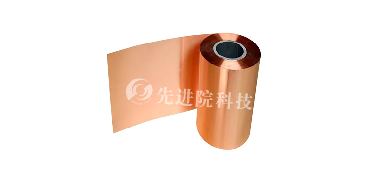
Bending resistant PI metal composite foilIn short, technology involves depositing nickel and copper layers on the surface of a PI substrate through a series of precision processes. The nickel layer, as the bottom layer, provides good adhesion and corrosion resistance, laying a solid foundation for subsequent copper layer deposition. The copper layer, with its excellent conductivity, greatly improves the signal transmission efficiency of wireless communication devices. The implementation of this technology not only solves the problem of poor conductivity of PI materials, but also endows the equipment with stronger environmental adaptability and longer service life.
1. Fine craftsmanship ensures quality: The PI nickel and copper plating process involves various high-tech methods such as electrochemical deposition and physical vapor deposition. Each step requires strict control of parameters to ensure the uniformity and density of the coating, thereby achieving the best electrical performance and protective effect.
2. Environmentally friendly and green manufacturing: While pursuing high performance, advanced institute technology also does not forget its environmental responsibility. It adopts environmentally friendly electroplating solutions and efficient recycling systems to reduce wastewater discharge and achieve green production.
3、 Innovate applications and open a new chapter in wireless communication
High adhesion nickel plated copper plated PI filmThe application of technology has brought significant performance improvement and cost optimization to wireless communication devices. In 5G and even future 6G communication networks, the transmission of high-frequency signals places higher demands on the conductivity and stability of components such as antennas and filters. Components using PI nickel and copper plating technology, with their excellent electrical performance and lightweight design, have become the key to improving the overall performance of communication equipment.
1. Efficient heat dissipation to ensure stable operation: In high-frequency and high-power working conditions, good heat dissipation capability is the key to ensuring stable operation of equipment. The PI copper plating layer not only enhances the thermal conductivity, but also effectively reduces the operating temperature of the equipment and extends its service life through clever combination with the heat dissipation structure.
2. Flexible design to meet diverse needs: The flexibility of PI materials enables wireless communication devices using this technology to achieve more complex and compact designs, meeting application requirements in different scenarios, such as wearable devices, IoT sensors, etc.
4、 Conclusion: Looking into the future, infinite possibilities
With the continuous maturity and popularization of PI nickel and copper plating technology, wireless communication devices are entering a new stage of development.Advanced Institute of TechnologyThe innovative practice not only demonstrates the deep integration of materials science and communication technology, but also opens up vast space for the future development of wireless communication field. We have reason to believe that in the near future, wireless communication devices based on PI nickel plated copper plating technology will connect every corner of the world with unprecedented efficiency, stability, and intelligence, opening a new era in human communication history.

 en
en  Español
 Français
 Português



